This course focuses on layered structures using the Ansys HFSS™ 3D Layout high-frequency electromagnetic simulation software in Ansys Electronics Desktop (AEDT)™ electronics systems design platform. Designed for brand new users, this course covers layer stackup, layout viewing, ports, vias, simulation boundary extents, layout driven assembly, hierarchy and cosimulation options.
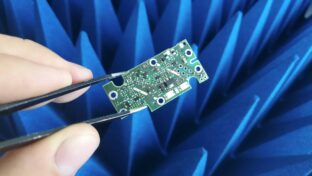
Workshops include a small differential via structure, a planar antenna array, an octagonal spiral inductor, a subdesign cutout from a printed circuit board with a BGA (ball grid array) mounted on it, and a full workflow example.
Learning Outcomes:
Following the completion of this course, you will be able to:
- Place ports, vias, and connect solder balls to ground planes.
- Configure circuits driving EM simulations hierarchically.
- Bring in external HFSS designs and position them in Ansys HFSS 3D Layout software.
- Create output variables for calculated quantities like quality factor.
- Set up FEM (finite element method) analyses in Ansys HFSS 3D Layout software.
- Generate and view results plots (post processing) of S-parameters.
Prerequisites:
- Any prior experience with Ansys HFSS EM simulation or Ansys Electronics Desktop RF circuit design, is helpful.
- Knowledge of high-speed digital circuit design, including S-parameters, transmission lines, and differential parts, is highly recommended.
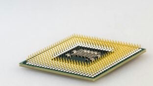
- Knowledge of printed circuit board design, including vias, component reference designators, and layer stackups, is valuable.
Please note: These training materials were developed and tested in 2025 R2 release.
-
Cost: $450.00
- Course Duration: 6+ HOURS
- Skill Level: Beginner
- Skills Gained: Learn layer stackup, placement of ports and vias, setup analysis and post-process results, hierarchy and cosimulation, in Ansys HFSS 3D Layout software.
No reviews available for this learning resource.