Premium
Electronics
Component Level Radiated Emissions using Ansys HFSS Software and Circuit With Mesh Fusion and Layout Component
$450.00
6+ HOURS
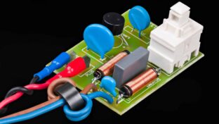
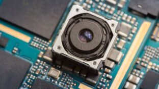
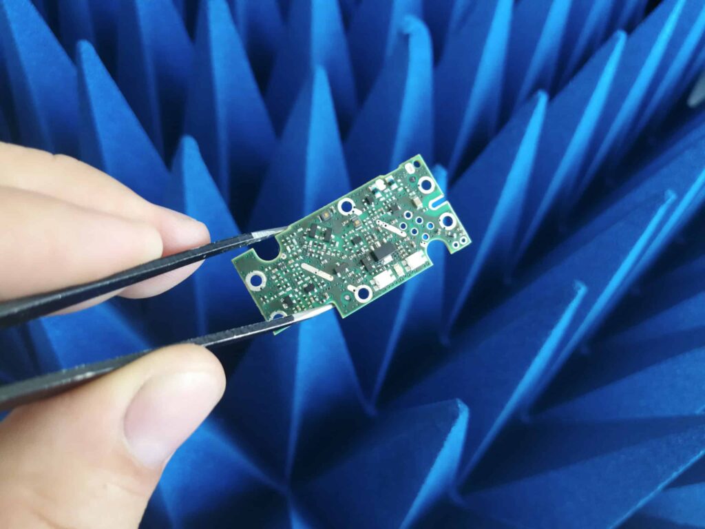
This course explores the topic of product’s radiated emissions testing where the RF emissions from the product are measured at a certain distance and compared to certain compliance limits. This includes the combined emissions from the PCB and the associated cables. It demonstrates an end-to-end workflow for component level radiated emissions (RE) including PCB, cable, test setup as per CISPR 25 and biconical antenna. This course includes the usage of Ansys HFSS™ high-frequency electromagnetic simulation software in Ansys Electronics Desktop (AEDT)™ electronics systems design platform.
Learning Outcomes:
Following completion of this course, you will be able to:
- Design RE test setup using HFSS modelling capabilities and leveraging 3D components, mesh fusion and layout component for the PCB.
- Understand the use of EMI Receiver probe to plot peak, quasi – peak and average emissions.
Prerequisites:
- Prior knowledge of Ansys HFSS design, boundary conditions, excitations, analysis setup and relevant parameters.
- Prior knowledge of Circuit Designer.
-
Cost: $450.00
- Course Duration: 6+ HOURS
- Skill Level: Expert
- Skills Gained: RE test setup, EMI receiver probe, Plot Emission report, 3D component, Mesh fusion, Layout component for PCB.
No reviews available for this learning resource.