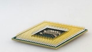

This course demonstrates and practices how to mount an IC package onto a printed circuit board (PCB) in HFSS 3D Layout in Ansys Electronics Desktop (AEDT)™ electronics systems design platform. The HFSS finite element (FEM) solver analyzes the combined structure and provides S-parameter results for the combined geometry. Additionally, there is a valuable appendix of information on multi-design projects in HFSS 3D Layout. This course complements existing HFSS 3D Layout training course workshops.
Learning Outcomes:
Following Completion of this course you will be able to:
- Learn a workflow for package on PCB simulation. Steps include setting up the ports on the package die, setting up the PCB ports, merging the package die onto the board, running the simulation and viewing the results.
Prerequisites:
- HFSS 3D Layout Getting Started course.
- Familiarity with signal integrity engineering principles such as differential pairs and transmission line insertion loss (S-parameters).
-
Cost: $450.00
- Course Duration: 1-2 HOURS
- Skill Level: Expert
- Skills Gained: PCB simulation, Setup ports on PCB, setup port on package die, Simulate and view results
No reviews available for this learning resource.