

Tagged: cinvestav, guest article, SCADE, scade suite, scade test, student
-
-
December 3, 2024 at 4:12 pm
 SolutionParticipant
Guest Article – Student – Three Phase Inverter with SCADE
This article is a guest contribution from Cinvestav. It was written by a student group as part of a Masters-level, semester long SCADE academic program course.
It explains the design and simulation of a system that controls a three-phase power inverter.
If you are an academic and are interested in teaching an engineering curriculum backed by Ansys tools, please have a look at our Ansys Funded Curriculum page.
Summary
Three-Phase inverters have long been used in various applications within power electronics and motor controllers, including brushless motor controllers (e.g. the same motors used in drones). Various methods to achieve a three-phase inverter exist, in this implementation we use a six-step controller to generate a three-phase response.
A six-step controller consists in switching three arrays of p-mos and n-mos, where the output voltage from each array is connected to a delta-resistor array. A controller for the six-steps were described using the MBD, also did the states of operation, the gate activation control and the handle of the operating frequency were disclosed here.
Three-Phase inverter
Brief description of the inverter is provided here:
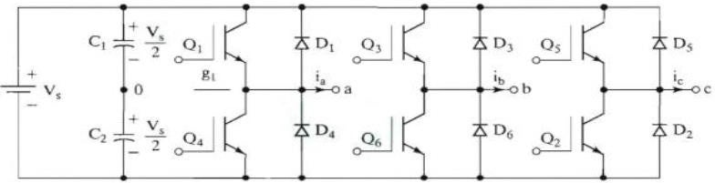
Illustration 1. Circuit Diagram of the inverterIn common applications, three-phase inverters are designed for high-power operations, being an effective solution for converting direct current (DC) to alternating current (AC) in industrial and power distribution systems. Three-phase inverters can be configured by connecting three single-phase bridge inverters in parallel, which can be half-bridge or full-bridge. This configuration allows for the creation of a balanced three-phase output, essential for powering three-phase motors and other high-power equipment.
There are two main classes of control signals that can be applied to the transistors in a three-phase inverter: 120° control and 180° control. The 180° configuration is more efficient in using the switches compared to the 120° configuration, as each transistor conducts for 180° of the signal cycle. In this configuration, there are always three transistors conducting at any given time, allowing for better resource utilization and higher system efficiency [1].
In detail, in the 180° configuration, each of the six transistors in the inverter is turned on for 180° of the electrical cycle. This means that there are always three transistors conducting current at any given time. This feature of the 180° configuration helps reduce switching losses and improves the overall efficiency of the inverter, as the time spent switching transistors on and off is minimized. Additionally, this configuration allows for a more uniform utilization of the transistors, prolonging their lifespan and improving system reliability.
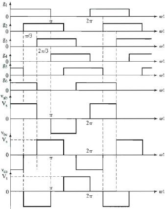
Illustration 2. Waveforms during 180 conductionsThe 120° configuration is also used in some three-phase inverters but is less efficient in terms of transistor usage. In this configuration, each transistor conducts for only 120° of the cycle, meaning that only two transistors are conducting current at any given time. This can lead to increased circuit design complexity and higher switching losses, reducing the overall efficiency of the inverter.
The waveforms produced by a three-phase inverter depend on the switching sequence of the transistors and the control configuration used. In the 180° configuration, the waveforms are smoother and have fewer harmonics, resulting in better power quality. This is especially important in industrial applications where power quality is critical for proper equipment operation.
Operation
The project consists of a 6 step three phase inverter, using the Model Based Design approach, this allows for a graphical and structured representation of the system, facilitating its understanding, simulation, and verification before physical implementation. SCADE is a suitable tool due to its ability to handle critical and complex systems, providing a robust environment for design and validation.
The inverter has two operating modes:
- Manual mode, the inverter frequency is controlled by an analog input provided by a joystick. This configuration allows for dynamic and continuous frequency adjustment, offering flexibility and quick response to user needs. The use of the joystick as an input interface is intuitive and practical, especially in applications where rapid and fluid frequency variability is required.
- Precision mode is designed for situations where more exact frequency control is required. In this mode, a button allows the current frequency of the inverter to be fixed, ignoring joystick signals. Once fixed, the frequency can be adjusted with greater accuracy using a pair of dedicated buttons.
This configuration is ideal for applications where frequency precision and stability are crucial, allowing the user to make fine adjustments without the inherent variability of analog joystick control.
In addition, while the system is powered, it must inform the user in which operating mode it is working.
The implementation of these two operating modes highlights the versatility and user- centered design of the system. In manual mode, adaptability and quick response are prioritized, while in precision mode, accuracy and detailed control are emphasized. This dual approach allows the inverter to adapt to different operational needs, improving its functionality and utility in various applications.
Requirements
Some requirements considered in the system are the following:
IN_HLR_BEH_01
The output signals shall be off when the system is turned on. Inver_State shall be established in OFF.
IN_HLR_ BEH _02
Inverter output signals shall turn on when the input Run/Stop value is true. Inver_State shall be established in ON_JOYSTICK.
IN_HLR_ BEH _03
The inverter shall be turned off when the Run/Stop input value is false. Inver_State shall be established in OFF.
IN_HLR_ BEH _04
The inverter shall maintain the last value of the frequency when the button Set is true.
Inver_State shall be established in ON_STEPS.
IN_HLR_ BEH _05
When the button Manual is pressed, the inverter shall respond to the input A0 and establish the frequency to the last value from input A0.
Inver_State shall be established in ON_JOYSTICK.
IN_HLR_ BEH _06
The inverter shall report when the system is on, but no mode has been selected. Inver_State shall be established in SLEEP.
System Implementation
Data types and constants
In Table 1 we find the enumerator declared for the identification of the system states.
Name
Definition
Comments and
InformationState
enum {STOP, RUN_STEPS, RUN_JOYSTICK, SLEEP}–
Table 2 shows the values of the constants that will be used in the system.
Name
Type
Value
Comments and
InformationMAX_BITSfloat324095.0–
PERIOD_INCfloat322.0–
PERIOD_MAXfloat32120.0–
PERIOD_MINfloat3210.0–
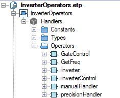
Call graph
Find below a call diagram showing the tree of created model operators. “inverter” is the root operator.
manualHandler operator
This operator is essential for the manual operation mode of the inverter, where the frequency is controlled by an analog input provided by a joystick. The “ManualHandler” is a process that uses the equation of a straight line to map the ADC (analog-to-digital converter) value of the development board, which varies between 0 and 4095, to the frequency change between the 6 steps of the inverter.
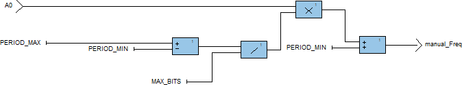
Illustration 3. manualHandler operatorThe implementation of the straight-line equation in the “ManualHandler” allows for a linear transformation of the ADC value to a suitable frequency for the inverter. This means that a direct and proportional relationship is defined between the analog input signal (the ADC value) and the desired output (the inverter frequency). In this way, the minimum ADC value (0) corresponds to the minimum operating frequency of the inverter, while the maximum ADC value (4095) is assigned to the maximum allowed frequency. This transformation ensures that frequency control is intuitive and precise, making it easy for the user to manipulate the inverter through the joystick and improving the system’s real- time functionality.
precisionHandler operator
The “precisionHandler” takes as its starting point the last frequency value mapped by the “ManualHandler” operator. From this base value, it allows incremental or decremental adjustments to be made to the output frequency.
This approach ensures that, once an initial frequency has been established through the joystick in manual mode, the user can make precise adjustments using a pair of dedicated buttons. These buttons allow the frequency to be increased or decreased in small steps, offering detailed and exact control that is critical for applications where precision is fundamental.
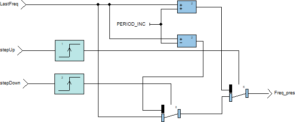
Illustration 4. precisionHandler operatorThe ability of the “precisionHandler” to maintain and adjust the frequency in an incremental manner ensures that the system can respond to the specific needs of different operating situations, providing both flexibility and accuracy in inverter control. This improves the system’s versatility and effectiveness, allowing for fine-tuned and precise adjustment that complements the dynamic variability provided by manual mode.
GetFreq operator
This operator is fundamental to determining the system’s mode of operation. This operator uses a conditional if block to evaluate the state of the control buttons and, based on this, activate the corresponding mode.
When the manual button is pressed, “GetFreq” activates the “ManualHandler” operator, changing the state variable to RUN_JOYSTICK. In this state, the system uses the analog input from the joystick to dynamically adjust the inverter frequency. If, instead, the Set button is pressed, ” GetFreq ” activates the “precisionHandler” operator, changing the state variable to RUN_STEPS. In this state, the system allows fine-tuned frequency adjustments through precise increments or decrements, ignoring the joystick signal.

Illustration 5.- GetFreq operatorIf no button is pressed, “GetFreq” enters a default state where the selected frequency is maintained as the last sampled value, and the state variable changes to SLEEP. This behavior ensures that, in the absence of new inputs, the inverter maintains its current frequency, providing stability and continuity in its operation. In this operator a “LimiterUnSymmetrical” was used to keep the parameter within the limits given in the requirements.
GateControl operator
The “GateControl” operator is a state machine designed with 6 distinct states, each indicating the logical state of the MOSFET gates implemented in the project. This operator is crucial for controlling the switching sequence of the MOSFETs, ensuring that they turn on and off in the correct order to generate the necessary three-phase outputs.
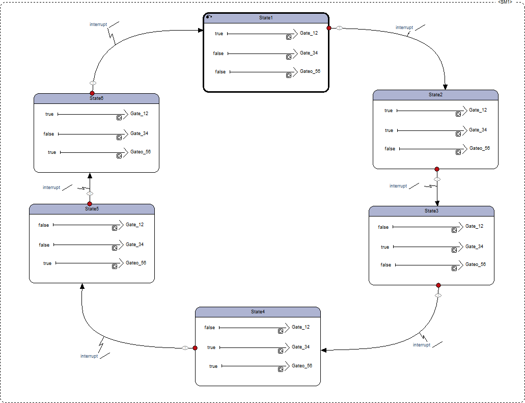
Illustration 6. GateControl operatorThe transition between these states is not arbitrary; it depends on a boolean value provided by the development board, which operates at a frequency determined by the operators described above, such as “ManualHandler” and “precisionHandler”.
These operators establish the switching frequency, and “GateControl” responds to this boolean value to change from one state to another. This synchronization ensures that the MOSFETs operate in a coordinated manner, producing the correct waveforms for each phase of the inverter.
InverterControl operator
The “InverterControl” operator is an implementation that manages the overall control of the inverter through a nested state machine structure. In the main state machine, “InverterControl” has two states: OFF and ON, which indicate whether the system is turned off or on. The transition between these states is controlled by the RUN button, allowing the user to turn the system on or off as needed.
Within the ON state, there is a second state machine that handles the detailed operation of the inverter. This sub-machine has two states: idle and GateControl. The transition between these states depends on the Set and Manual buttons.
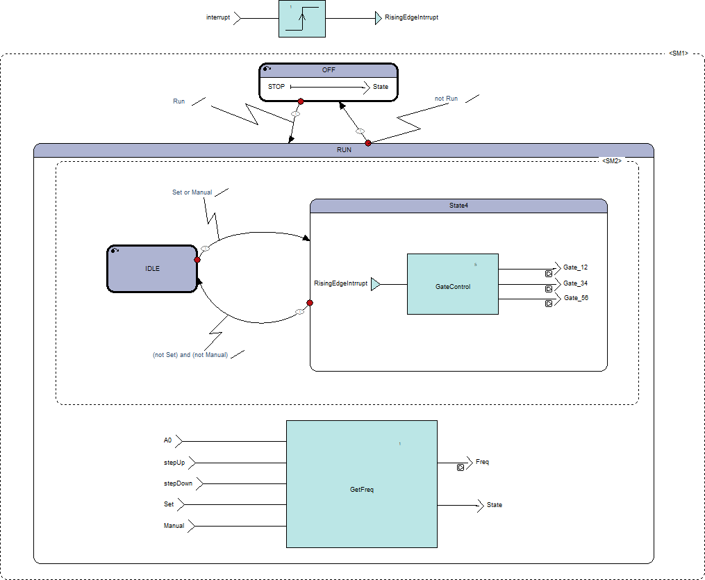
scade-029-invertercontrol.pngIn parallel with this sub-machine, and within the ON state, the “GetFreq” operator operates. This operator determines the mode of operation based on the buttons pressed, selecting between manual adjustment and precision modes, and ensuring that the inverter responds appropriately to user inputs.
Inverter operator
As the top-level block, the “inverter operator” integrates and coordinates the functions of all the subcomponents of the system. The inputs to the operator are internally connected to various operators such as “ManualHandler”, “precisionHandler”, “getFreq”, and “GateControl”, each of which handles a specific part of the control and operation of the inverter. These internal connections ensure that each operator receives the necessary signals and data to function correctly. The outputs of the “inverter operator” provide the expected values that control the frequency and switching sequence of the inverter. These outputs are derived from the integration of the results of the internal operators, ensuring that the system operates in a coherent and efficient manner.
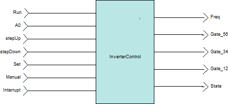
Illustration 8. Inverter operatorSimulation
From illustration 9, a crucial part of the simulation of the 6-step three-phase inverter control system is shown. In this image, the inverter state indicates that it is in SLEEP mode. This state is significant because it reveals that, although the system is on, no specific operating mode has been selected.
SLEEP mode is activated when both the Set button and the Manual button are in a boolean false state. This implies that they have not been pressed, leaving the system in an inactive state but ready to receive commands. The design of this state aims to provide a safe and stable condition in which the system does not perform any active operation on the MOSFETs, thus avoiding any unwanted switching that could cause problems in the hardware or connected load.
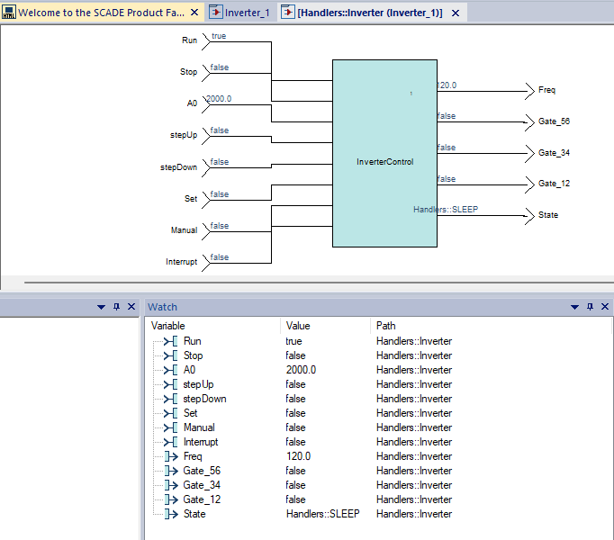
Illustration 9. System in sleep stateIn illustration 10, the Manual button has changed to a logical high state, causing the inverter state to change from SLEEP to RUN_JOYSTICK. This state change is crucial because it indicates that the system has received an active input and is now in manual operation mode.
With the Manual button in a logical high state, the “getFreq” operator detects this condition and transitions to the RUN_JOYSTICK state. In this mode, the system begins to use the analog input A0 from the joystick to control the inverter frequency. The “ManualHandler” operator is responsible for processing this input, mapping the received value of 0-4095, given by the ADC of the development board, to a corresponding frequency that will be applied to the switching of the MOSFETs.
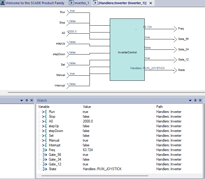
Illustration 10. System in RUN_JOYSTICK stateIn illustration 11, the state of the Manual button has been changed to false and the Set button to true, causing the system state to transition to precision mode, also known as RUN_STEPS.
When the Set button is activated (logical high state), the “getFreq” operator detects this condition and changes the inverter state from RUN_JOYSTICK to RUN_STEPS. In this mode, the system ignores the analog input from the joystick and instead uses the “precisionHandler” operator to control the inverter frequency. This operator takes the last frequency value mapped by “ManualHandler” and allows the user to make precise increments or decrements to the frequency using a specific pair of buttons.
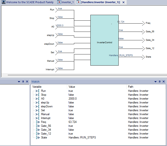
Illustration 11. System in RUN_STEPS stateVerification
Using the SCADE testing tool, the necessary scenarios were performed to verify the system’s operation. These tests were designed to stimulate the system’s inputs in all possible states, ensuring that each expected transition and behavior occur correctly and in accordance with the specifications.
In illustration 12, a crucial test of the system is shown, focused on the state machine of the “GateControl” operator. This test was designed to ensure that the inverter transistors are activated correctly and in sequence, as their precise operation is essential for generating an adequate three-phase sinusoidal signal.
# toggle the gates

SSM::set     Interrupt       true
SSM::cycle
SSM::set     Interrupt       false
SSM::cycle

SSM::set     Interrupt       true
SSM::cycle
SSM::set     Interrupt       false
SSM::cycle

SSM::set     Interrupt       true
SSM::cycle
SSM::set     Interrupt       false
SSM::cycle

SSM::set     Interrupt       true
SSM::cycle
SSM::set     Interrupt       false
SSM::cycle

SSM::set     Interrupt       true
SSM::cycle
SSM::set     Interrupt       false
SSM::cycle

SSM::set     Interrupt       true
SSM::cycle
SSM::set     Interrupt       false
SSM::cycle
Illustration 12. Test for “GateControl” operator
In illustration 13, specific tests are presented for two of the critical states of the 6-step three-phase inverter control system: the STOP state and the RUN_STEPS state. These tests are fundamental to ensuring that the system responds correctly in these key operating conditions.
# Stop the inverter operations

SSM::set Manual false
SSM::set Run    false
SSM::set Stop   true
SSM::check State Handlers::STOP sustain=5
SSM::cycle 5
SSM::cycle

# Run steps

SSM::set Stop   false
SSM::set Set    true
SSM::set Run    true
SSM::cycle
SSM::set stepDown   false
SSM::set stepUp   true
SSM::cycle

SSM::check State Handlers::RUN_STEPS sustain=5
SSM::cycle 5
SSM::cycle
Illustration 13. Test for the RUN_STEPS and STOP state.
Coverage
In Table 3, the system coverage summary table is presented, which is the result of the tests performed using the SCADE testing tool.
The coverage table provides a detailed summary of the test results, indicating the percentage of coverage achieved in different components and states of the system
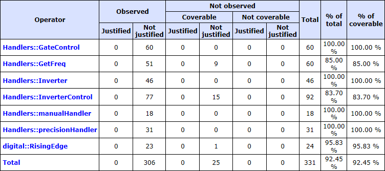
Table 3. Coverage.Physical Implementation
The system will be implemented on an NXP k64 development board in the MCUXpresso development environment using the following electronic components:
- IRF9540N MOSFET as P part of the inverter
- IRF530N MOSFET as N part of the inverter
- TIP41C TRANSISTOR to switch to higher voltage
- Joystick as analog input to the system and manual mode control
- push buttons to turn on the system and change operating modes
- Nokia5110 LCD to show the user the current operating mode
In illustration 14, the configuration of the inverter circuit mounted on a protoboard is shown. This circuit uses P-type and N-type MOSFETs, whose gates are connected and activated by a power transistor. This transistor is, in turn, switched by the system’s microcontroller, allowing for precise control of the output signal.
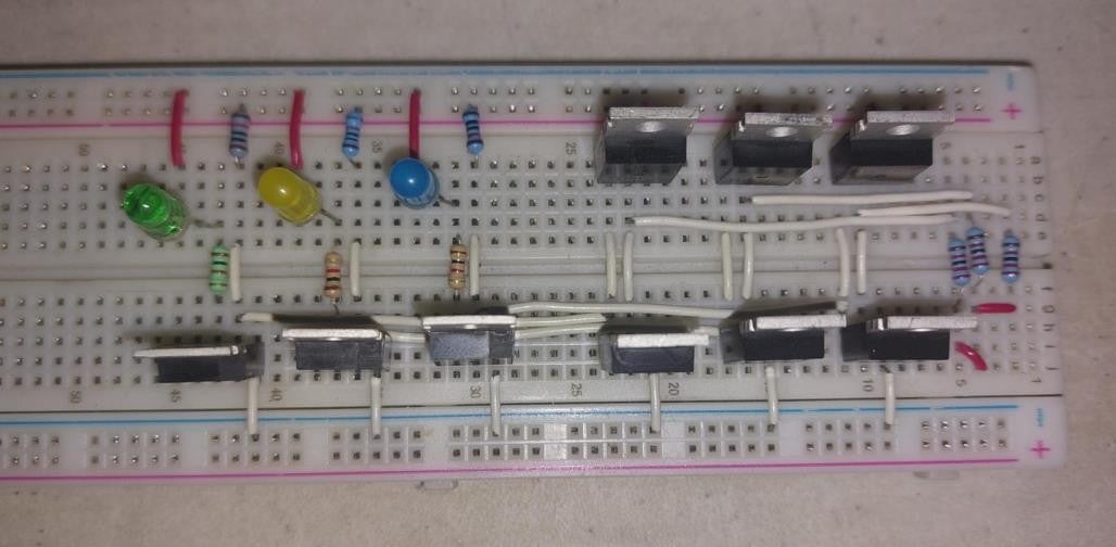
Illustration 14. Inverter circuitIn illustration 15, the circuit of the button panel connected to the microcontroller and the LCD screen is shown, which allows the user to interact with the system and visualize the current state of the inverter. This configuration is essential for controlling and monitoring the system in real-time, in addition to being part of the software requirements.
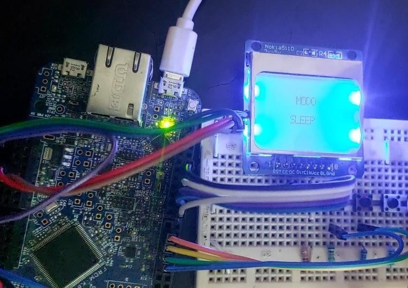
Illustration 15. Circuit of the button panel and LCD.In illustration 16, the system is shown in operation, being monitored on an oscilloscope. Here, the inverter output is verified, and it is ensured that it is operating correctly under manual control. In particular, the output signal is shown with the system’s minimum frequency, controlled via manual mode.
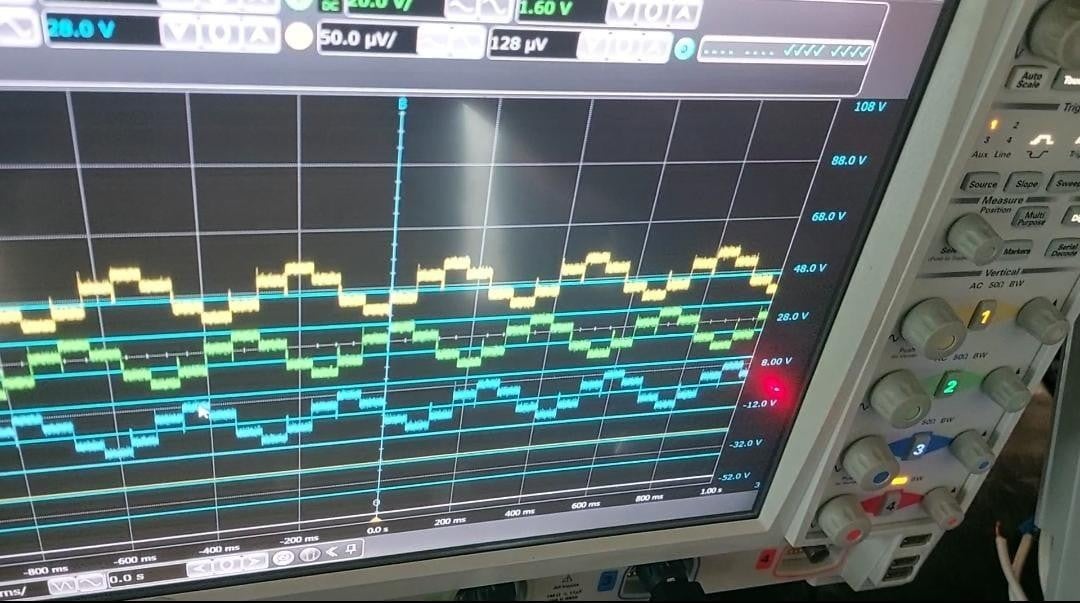
Illustration 16.- Three-phase signal on oscilloscope at minimum frequencyThe illustration 17 shows the same case but with the maximum possible frequency. In both, a correct displacement between phases is observed, so it can be implemented in low power applications without difficulties.
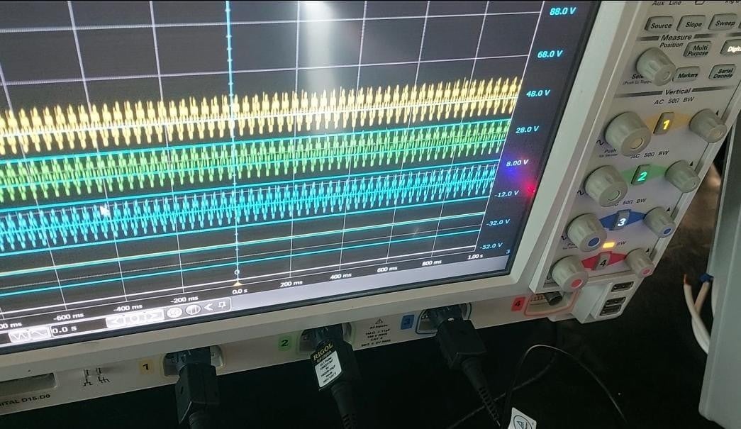
Illustration 7. Three-phase signal on oscilloscope at maximum frequencyFeedback on MBD and SCADE
The use of Model Based Design along with the SCADE tool has proven to be an effective methodology for the development and validation of the 6 steps three phase inverter system. The ability to design and simulate the system at the model level has allowed for a clear and precise definition of the inverter’s requirements and behaviors. By employing SCADE, a seamless integration of the different operators and components of the system has been achieved, facilitating the validation and optimization of the design. The simulation of behavior in different operating modes, such as manual and precision, has been key to ensuring that the system meets the specifications and functions correctly in real world conditions.
Furthermore, the implementation of the MBD methodology in combination with SCADE tools has optimized the testing and verification process. The ability to perform tests and obtain complete coverage in all evaluated metrics has ensured that the system is robustly validated before its physical implementation.
References
[1] Rashid, M. H. (2022). Electronica De Potencia Circuitos Dispositivos Y Aplicaciones (3.a ed.). PRENTICE HALL/PEARSON
https://riverraid17.files.wordpress.com/2010/03/electronica-depotencia-rashid-espanol.pdfAbout the authors

Pablo Daniel Pérez Montes (LinkedIn) is soon to graduate as a Communications and Electronics Engineer from Centro Universitario de Ciencias Exactas e Ingenierías (CUCEI) in Guadalajara, Mexico. He is strongly committed to Digital Design and the development of Electronics Systems which involves Embedded both Hardware and Software solutions. Currently, he is gaining professional experience in the IT areas, such as Telecom and networks, however, he’s set to develop his career into the silicon industry.

Eduardo Mateo Martínez Solís (LinkedIn) graduated as a Communications and Electronics Engineer from the Centro Universitario de Ciencias Exactas e Ingenierías (CUCEI) in Mexico. His interests are focused on embedded systems, digital verification, and the development of efficient and reliable solutions. Currently, he has experience in manufacturing and testing processes, which include implementing methodologies to ensure product quality and carrying out validation and diagnostic procedures for electronic systems.
-


Introducing Ansys Electronics Desktop on Ansys Cloud
The Watch & Learn video article provides an overview of cloud computing from Electronics Desktop and details the product licenses and subscriptions to ANSYS Cloud Service that are...

How to Create a Reflector for a Center High-Mounted Stop Lamp (CHMSL)
This video article demonstrates how to create a reflector for a center high-mounted stop lamp. Optical Part design in Ansys SPEOS enables the design and validation of multiple...
Introducing the GEKO Turbulence Model in Ansys Fluent
The GEKO (GEneralized K-Omega) turbulence model offers a flexible, robust, general-purpose approach to RANS turbulence modeling. Introducing 2 videos: Part 1 provides background information on the model and a...

Postprocessing on Ansys EnSight
This video demonstrates exporting data from Fluent in EnSight Case Gold format, and it reviews the basic postprocessing capabilities of EnSight.

- An introduction to DO-178C
- ARINC 661: the standard behind modern cockpit display systems
- Scade One – Bridging the Gap between Model-Based Design and Traditional Programming
- Scade One – An Open Model-Based Ecosystem, Ready for MBSE
- SCADE and STK – Satellite Attitude Control
- Scade One – A Visual Coding Experience
- Using the SCADE Python APIs from your favorite IDE
- Introduction to Formal Verification and SCADE Suite Design Verifier
- Efficient Development of Safe Avionics Software with DO-178C Objectives Using SCADE Suite
- How to integrate multiple SCADE models into one executable

© 2026 Copyright ANSYS, Inc. All rights reserved.
