-
-
July 4, 2022 at 6:59 am
 Watch & LearnParticipant
This signal integrity video explores unwanted mode conversion, from differential signal to common signal, due to unbalanced ground return current via paths in a multilayer differential pair simulated in HFSS 3D Layout. Starting at 1:35, the video shows how to move a differential pair, including the port, from one lower layer up to another layer in one operation. At 2:46 the video describes the engineering relation between asymmetry and mode conversion in terms of mixed mode S-parameters. The HFSS 3D Layout unbalanced (asymmetric) design, with a ground return path via missing, is created after 4:58. The change to an HFSS fully arbitrary 3D (FA3D) design starts at 7:19, with the symmetrical S-parameters shown at 8:34. The asymmetrical (unbalanced) FA3D design consideration starts at 9:14
-


Introducing Ansys Electronics Desktop on Ansys Cloud
The Watch & Learn video article provides an overview of cloud computing from Electronics Desktop and details the product licenses and subscriptions to ANSYS Cloud Service that are...

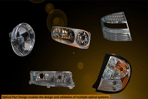
How to Create a Reflector for a Center High-Mounted Stop Lamp (CHMSL)
This video article demonstrates how to create a reflector for a center high-mounted stop lamp. Optical Part design in Ansys SPEOS enables the design and validation of multiple...

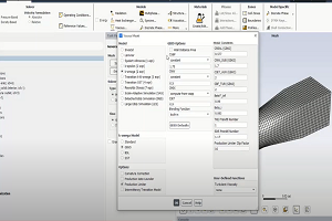
Introducing the GEKO Turbulence Model in Ansys Fluent
The GEKO (GEneralized K-Omega) turbulence model offers a flexible, robust, general-purpose approach to RANS turbulence modeling. Introducing 2 videos: Part 1 provides background information on the model and a...

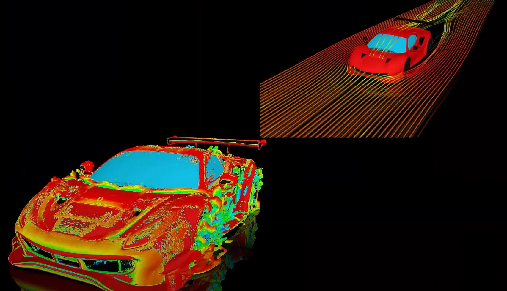
Postprocessing on Ansys EnSight
This video demonstrates exporting data from Fluent in EnSight Case Gold format, and it reviews the basic postprocessing capabilities of EnSight.

- How do I calculate inductance and resistance of a coil in post-processing phase?
- How to create and manage a queue of simulations?
- How to import/export an Ansys Maxwell model in Workbench?
- How to enable GPU acceleration in Electronics Desktop?
- Are solid losses and eddy losses the same in Maxwell?
- Electric Motor Design Using Ansys Motor-CAD – Part 1
- How to fix messed up Windows layout?
- What are the available boundary conditions in Maxwell?
- How to calculate capacitance and inductance in Maxwell Transient solver?
- How to perform a material sweep?

© 2025 Copyright ANSYS, Inc. All rights reserved.


