Ansys Assistant will be unavailable on the Learning Forum starting January 30. An upgraded version is coming soon. We apologize for any inconvenience and appreciate your patience. Stay tuned for updates.
Electronics

Electronics

Topics related to HFSS, Maxwell, SIwave, Icepak, Electronics Enterprise and more.

S21 results missing in 100GHz Metamaterial simulation with Floquet Ports

    • arakawa-taro-vj
      Subscriber

      Hello,

      I am a graduate student researching "Metamaterial Antenna-Integrated Quantum Well Optical Modulators" for the 100GHz band. I am currently facing an issue where S21 is not being output (or appears as zero) in my HFSS simulation, while S11 is plotted correctly.
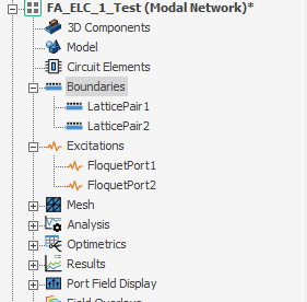
      Simulation Setup:

      Frequency: 100GHz (W-band)

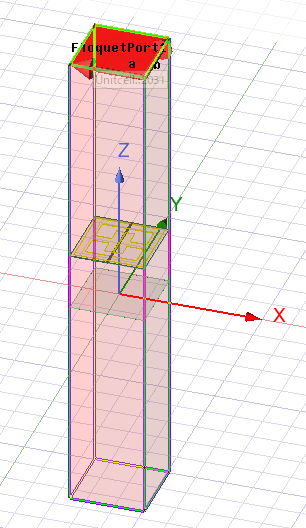
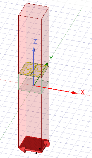
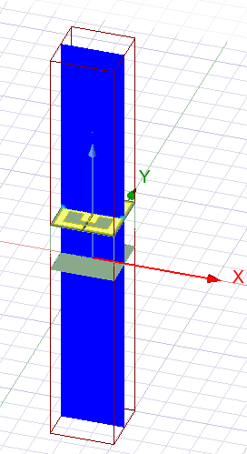
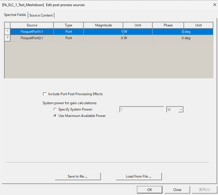
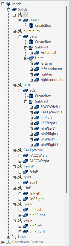
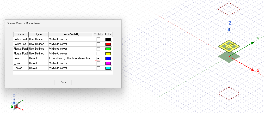
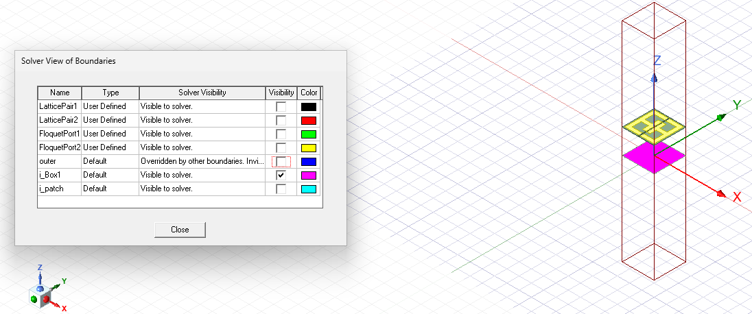
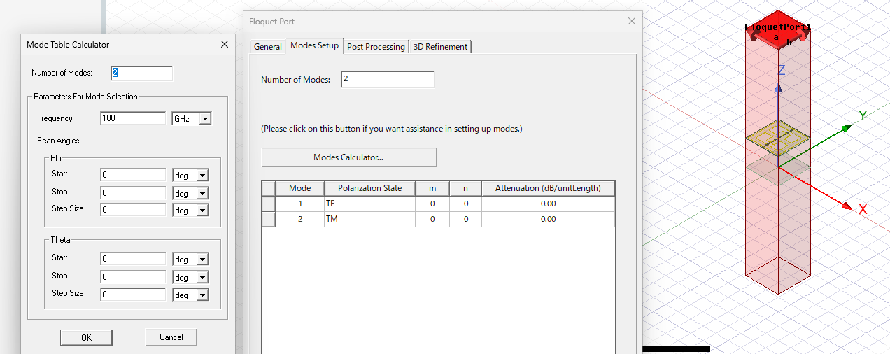
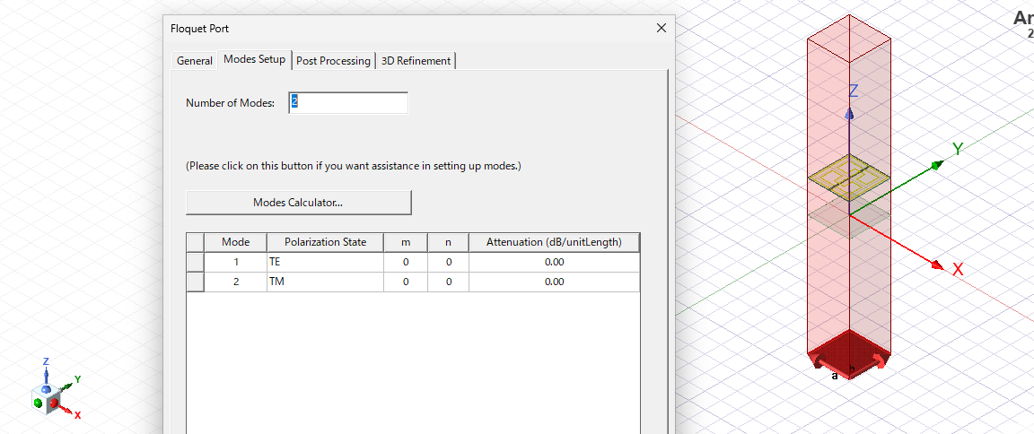
      Ports: Floquet Ports (Port 1 and Port 2)

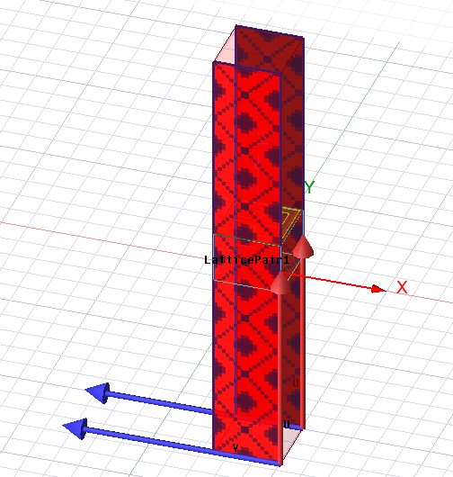
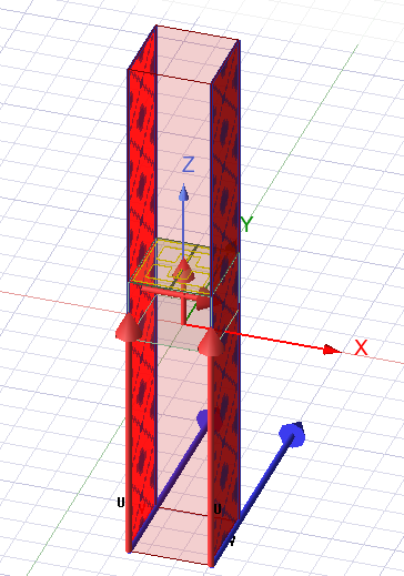
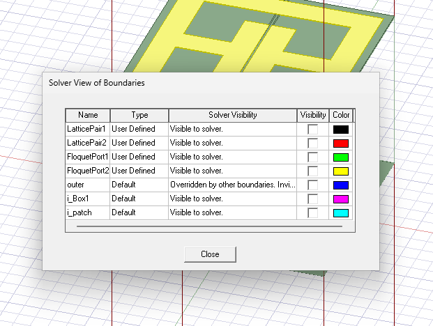
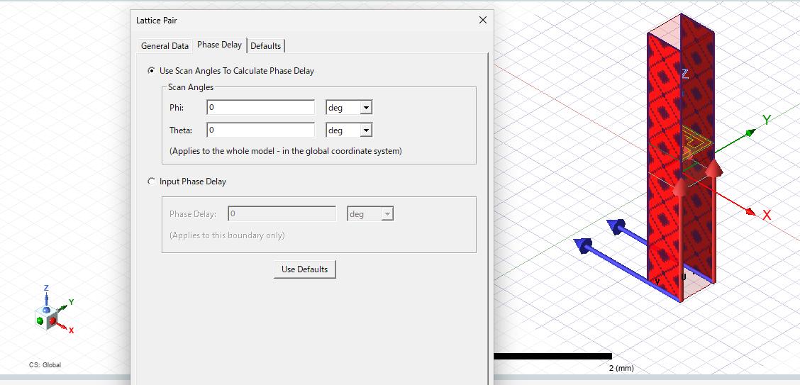
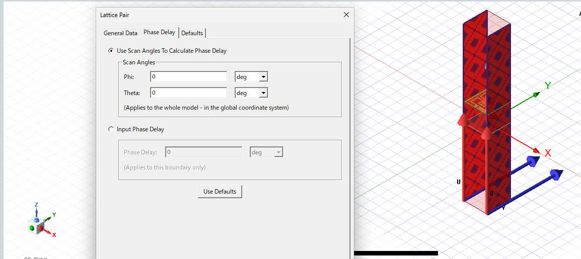
      Boundaries: Primary/Secondary (Master/Slave) Periodic Boundary Conditions

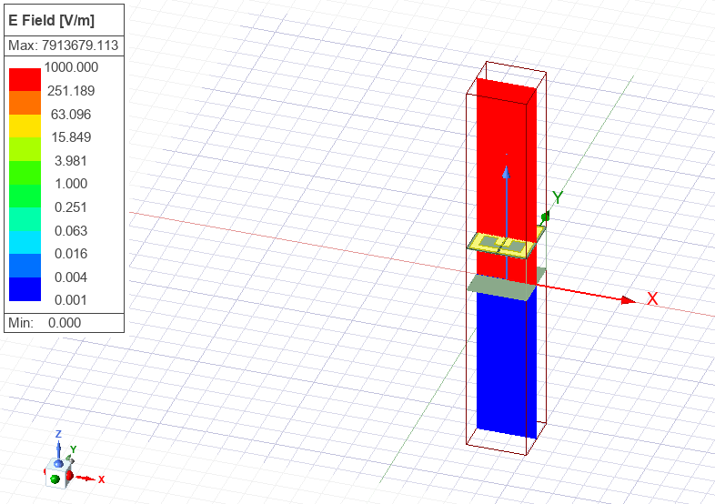
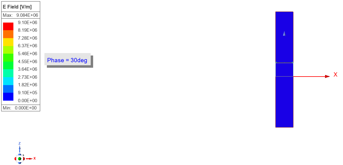
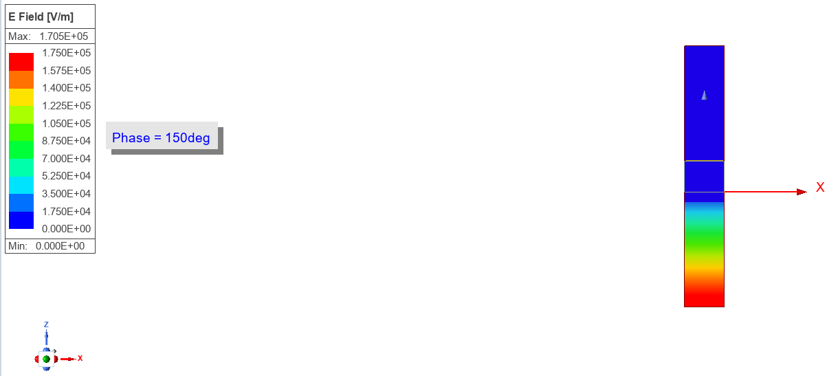
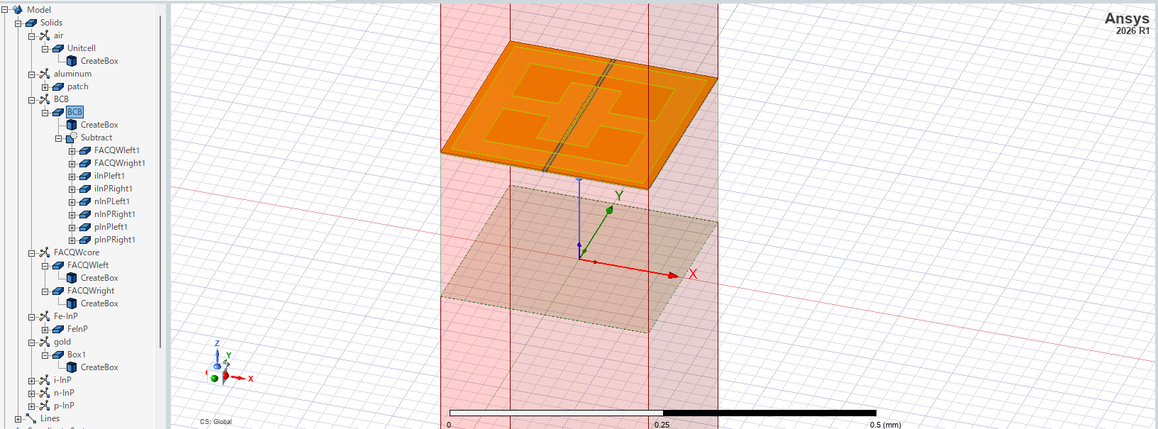
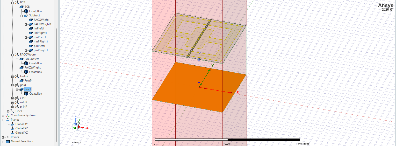
      Structure: A metamaterial resonator (Meta-atom) coupled with a semiconductor waveguide (FACQW core layer).
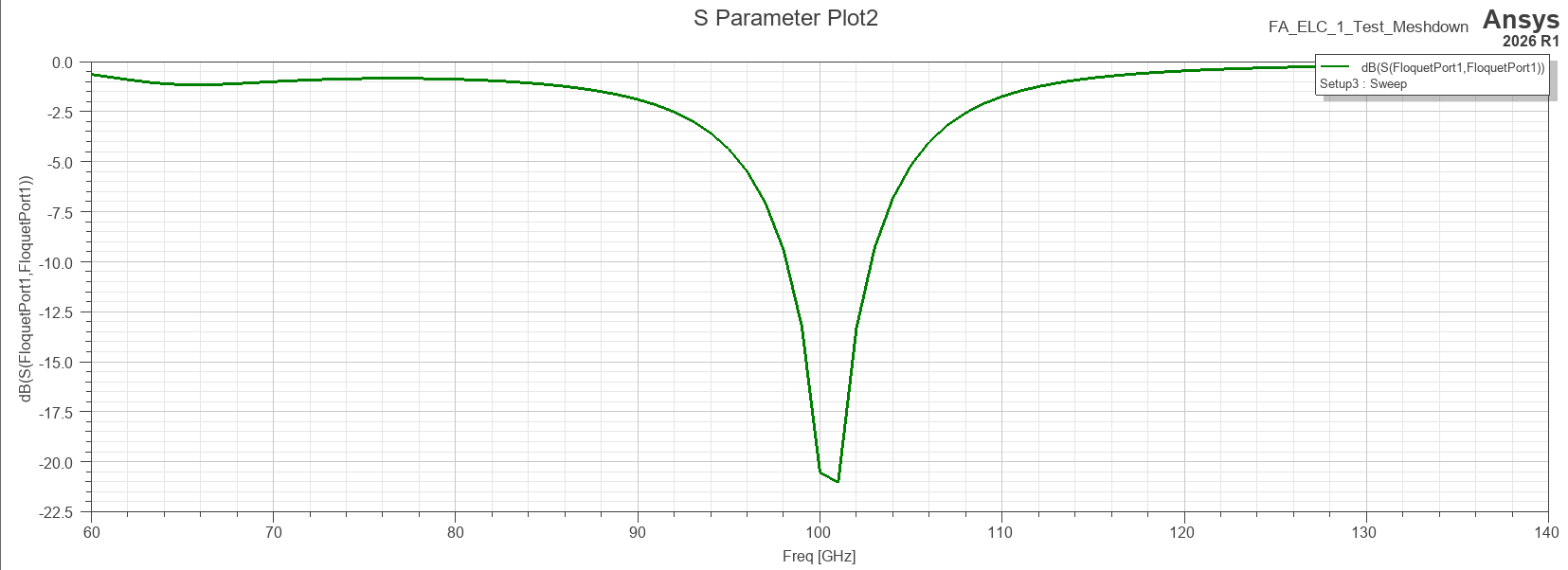
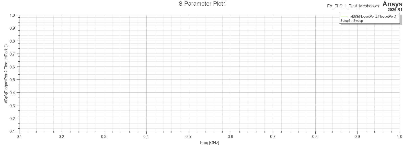
      Current Issue:
      Despite successfully running the analysis, only S11 data is available in the Results. S21 remains at zero or is missing from the plot options altogether.

      What I have tried:

      Benchmarking: I successfully reproduced the S-parameter results of a previous study using a similar setup with a Lithium Niobate (LN) substrate.

      Material Check: I suspected the high-dielectric waveguide might be the cause, but changing the waveguide material/dimensions did not resolve the missing S21 issue.

      Port Modes: I have checked that both Floquet ports have the same number of modes defined.

      Questions:

      Could this be an issue with the "Post Processing" mode setup in the Floquet port settings?

      Are there specific conditions where S21 is not calculated even if the simulation completes without errors?

      Could the polarization setup between the two ports be causing an orthogonality issue that nullifies the transmission?


    • Gia
      Ansys Employee

      What is the 2D square object centered at the [x,y,x] origin?

      To help debug, please select the XZ plane from the 'Planes' section of the model tree and then click [HFSS > Fields > Plot Fields > E > Mag_E]. - Do you see EM fields being plot thorughout the entire unit cell?

    • arakawa-taro-vj
      Subscriber

      Thank you for your response.
      When I plotted the XZ plane, the result looked like the figure below.
      Does this mean that the issue isn’t with the port, but rather that electromagnetic waves aren’t entering the device in the first place?

    • Gia
      Ansys Employee

      Double-click on the colorbar in the plot legend - then adjust the min to 1e-3, the max to 1e3, and then set the scale from 'linear' to 'log'.

      You can also change which port is being excited in the field plots by right-clicking on 'Excitations' in the project tree and then selecting 'Edit Sources' - here you can scale the field plots based on the magnitude and phase being input into each port.

      What is the height of the air space modeled above the metamaterial structure? - There should be at least lambda/4 distance to allow the wave to propigate from the Floquet port.

    • arakawa-taro-vj
      Subscriber

      Thank you for your response.
      First, please see the graph below showing the electromagnetic field distribution on a logarithmic scale.
      As a fully passive device, do you think these results are reasonable?

      In addition, the command displayed via “Edit Source” is as follows.
      If the configuration specifies that 1 W of electromagnetic radiation is incident from port 1, this setting appears to be correct.

      The height of the air layer is 750 μm from the device surface, which is approximately one-quarter of the wavelength.

      If electromagnetic waves are being properly incident on Port 1, I believe Port 2 is the reason why S21 is not being output, but I have not yet found any evidence to support this.

    • Gia
      Ansys Employee

      Adjust the max of the scale to 1e7 to get a better view of the fields. - Right-click on the plot's name and select 'Animate' and then use the default options. - You should see how the fields propigate as a function of the input excitation's phase.

      Next - Change the edit sources setting so that you are only exciting port 2 - then view/animate the fields.

      What is the 2D square object centered at the [x,y,x] origin? - It looks like you have a sheet of metal there? - This would block any transmission across the structure...

    • arakawa-taro-vj
      Subscriber

      First, when Port 1 is excited, the result is as shown in the figure below, with only the electromagnetic field near the antenna changing.

      Next, when Port 2 was activated, changes in the electromagnetic field were observed across the entire bottom surface of the device.

      Also, the green object near the origin is a 3D object made of an insulating film called BCB. Since it is not a metal, it is unlikely to be obstructing the light.

    • Gia
      Ansys Employee

      It looks like you only have the Floquet ports set to solve for 1x single mode each. - So it is possible that you could be exciting the TE mode with one port and the TM mode with the other.

      Please review the HFSS help PDF regarding use of the floquet modes calculator (that is found within the floquet port settings UI) to make sure you are solving for all the possible modes that could propigate.

      Additionally, as a side note, I would reccomend taking some time to adjust the field plot bounds in order to get a better view of the field propigation. - Try to adjust both the upper and lower bounds so that neither the red nor blue extremes of the scale are saturating.

    • arakawa-taro-vj
      Subscriber

      Thank you for the advice.

      I have set the number of modes to 2 for both Floquet ports to observe mode conversion, but unfortunately, S21 still shows no transmission for either mode.

      Given that the fields are concentrating around the meta-atom but not reaching Port 2, I suspect a fundamental issue with the structure or the boundary setup rather than a mode-matching issue.

      Could you please advise if I should check the following possibilities?

      Lattice Vector/Pair orientation: Is it possible that a mismatch here is causing the ports to 'see' a short circuit or an invalid boundary?

      Object definition: As I mentioned, the green square is BCB, but could the solver be interpreting it as a PEC surface if it's modeled as a 2D sheet?

      Boundary conditions: Are there any specific conditions in the 'Lattice Pair' settings that might be unintentionally blocking the propagation?

      Any guidance on what to check in the model tree to rule out these physical blockages would be greatly appreciated.

    • Gia
      Ansys Employee

      To view an overlay that shows which boundaries/materials are assigned to each structure, right-click once on the HFSS design name in the project tree and then select 'Boundary Display (Solver View)'

      To help better diagnose, please post screenshots of the model tree with all solid and sheet objects expanded. - Also, please post screenshots of the material properties for any custom material definitions.

    • arakawa-taro-vj
      Subscriber

      Understood.
      The Boundary Display is now as follows.

      The contents of the object tree are as follows.

      The parameters for custom material properties are as follows:

      We apologize for the inconvenience, but we would appreciate your assistance with the diagnosis.

    • Gia
      Ansys Employee

      Thank you - Can you also please post screenshots of the model with the boundary solver view overlay enabled for each: 1)'outer', 2) 'i_Box1', and 3) 'i_patch'? And also a screenshot + description of each of your boundaries assigned as listed/shown in the Project Manager tree on the far left of the UI?

      Also, I apologize for the many steps required here - we are not allowed to send/recieve/review model files and we can only review images that users post here but we cannot post any images.

    • arakawa-taro-vj
      Subscriber

      The screenshots of the model are as follows.

      FloquetPort was installed at the top and bottom for S-parameter analysis and plane-wave incidence.

      LatticePair was configured as an infinitely arrayed module with periodic boundary conditions in the X and Y directions.
      No settings other than the direction of the lattice vectors were changed.

      Please let me know if anything is unclear.

    • Gia
      Ansys Employee

      What type of boundary do you have assigned to 'i_Box1'  and  'i_patch'? - They are listed in the project tree on the far left of the UI.

    • arakawa-taro-vj
      Subscriber

      The boundary looks like the image shown here.
      Does this mean that, like FloquetPort, we need to set boundary conditions for “i-Box” and “i-patch” as well?

    • Gia
      Ansys Employee

      Thank you - It appears that the object 'Box1' is not assigned to be the BCB material - it is assigned as 'gold'.

      Gold is a very good conductor and so this solid piece of gold material is blocking any transmission of energy through the model.

      Please try re-assigning 'Box1' as BCB and then re-solve the model.

    • arakawa-taro-vj
      Subscriber

      I have re-verified my material assignments:

      The object 'BCB' (under the 'BCB' folder) is correctly assigned as the 'BCB' material (Dielectric).

      The object 'Box1' (under the 'gold' folder) is the ground electrode, assigned as 'gold' (Metal).

      They are physically distinct components. Could you please clarify which object you believe is incorrectly assigned as gold? Is it possible that 'Box1' is overlapping with the unit cell boundaries, causing the transmission blockage?

    • Gia
      Ansys Employee

      Can you please post screenshots which in each image includes both the model tree and model view windows for the following two objects?

      1) Select the gold object 'Box1' in the model tree to highlight this object in the model view window

      2) Select the BRB object 'BRB' in the model tree to highlight this object in the model view window

    • arakawa-taro-vj
      Subscriber

      Does BRB stand for BCB?
      I’ve attached an image below showing the BCB and gold objects.

      Would it be reasonable to assume that the current is not passing through the port, but rather is being blocked by the gold in the BCB or ground electrode?

    • Gia
      Ansys Employee


      As I had suspected in my previous posts on [May 13, 2026 at 10:07 pm] and [May 15, 2026 at 4:37 am], the “the 2D square object centered at the [x,y,x] origin” is the issue.

      Unit cells model an infinite array of adjacent cells in both lattice pair directions. – A solid sheet of gold here results in an infinitely large 2D sheet of conductor. – Electric fields cannot penetrate a solid conductor at high frequencies due to the skin effect – so this gold object forms what may be considered a ‘Faraday Cage’ – which will block any tranmission of signal between the Floquet ports.


    • arakawa-taro-vj
      Subscriber

      After reducing the size of the ground electrode, the S-parameters were calculated.
      As you pointed out, it appears that the gold module was obstructing transmission.
      Thank you very much for your guidance!

Viewing 20 reply threads
  • You must be logged in to reply to this topic.
[bingo_chatbox]