Hello,
I have an HFSS design which consists of a radiating patch, a delay line, coupled boundries, and a floquet port excitation. The patch is connected to the delay line through a PIN diode. Ideally, the reflection phase at the floquet port (i.e., ang_deg(S(1,1))) should have a 180° difference when the state of the diode changes from forward to reverse bias.
To simulate the PIN diode under forward and reverse bias conditions, I use two lumped ports that are linked to a Circuit design. In the Circuit design, I added two identical subcircuit elements that are linked to the original HFSS design. The HFSS subcircuit elements are 3 port elements (i.e., Port 1 = Floquet port mode #1, Port 2 = Lumped port #1, and Port 3 = Lumped port #2). In Port 1 I add a microwave port with free-space impedande to simulate the floquet port. For Ports 2 and 3, I add a 2-port compenent which is linked to the touchstone file of the PIN didode under the two conditions (see the figure below).
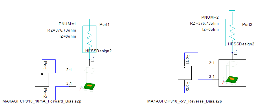
With this setup, the microwave ports, "Port1" and "Port2", represent the floquet port of the element when the PIN diode is forward and reverse biased, respectively. Therefore, the ideal element design should produce results where "ang_deg(S(Port1,Port1))" and "ang_deg(S(Port2,Port2))" are 180° out of phase.
I would like to use Optimetrics in the Circuit design to optimize the dimensions of the patch and delay line so that there is a 180° phase difference between "ang_deg(S(Port1,Port1))" and "ang_deg(S(Port2,Port2))". However, this is challenging because adjusting these will effect the mutual coupling with the neighboring elements that are modeled using periodic boundary conditions. Therefore, the HFSS subcircuit links should be updated after each iteration in the optimization process to account for the effect of mutual coupling. Is there anyway to run an Optimetrics optimization in Circuit design that updates the linked HFSS subcircuit elements after each iteration?
Specifically, I would like to run a Quasi Newton (Gradient) optimization with the following cost function: abs(ang_deg(S(Port1,Port1)) - ang_deg(S(Port2,Port2))) = 180°.
Thank you for your help!


