Ansys Assistant will be unavailable on the Learning Forum starting January 30. An upgraded version is coming soon. We apologize for any inconvenience and appreciate your patience. Stay tuned for updates.
Electronics

Electronics

Topics related to HFSS, Maxwell, SIwave, Icepak, Electronics Enterprise and more.

HFSS+Nexxim co-simulation for GCPW-fed active antenna with amplifier

    • r13942107
      Subscriber

      Hello everyone,

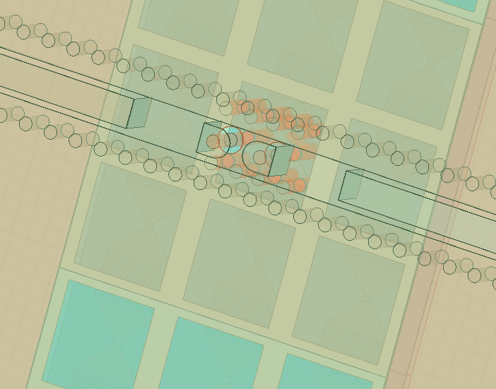
      I am currently working on a millimeter-wave Antenna-in-Package (AiP) co-design using:

      • HFSS 3D EM
      • Ansys Circuit / Nexxim
      • Differential GCPW feed
      • IPD antenna
      • Distributed Amplifier (DA) S2P model

      The system architecture is:

      Connector
      → Differential GCPW
      → DA
      → Differential GCPW
      → Signal vias
      → IPD antenna

      My goal is to obtain:

      • Active antenna gain
      • Active radiation pattern
      • Far-field results including the DA gain, phase, and mismatch effects

      I would like to ask:

      1. If the goal is to obtain the active radiation pattern including amplifier effects, what is the recommended workflow?
      2. Is the correct approach:

      HFSS simulates only the antenna + feed structure
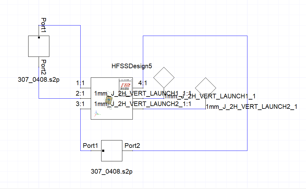
      → dynamic link to Circuit/Nexxim
      → insert the DA S2P model in Circuit
      → solve the active far-field pattern from Circuit/Nexxim?

      1. For the differential GCPW feed, which port type is more appropriate at the DA insertion location?
      • Lumped port
      • Circuit port
      • Wave port
      1. Also, what is the correct method to simulate and obtain:
      • Active antenna gain
      • Active radiation pattern
      • Far-field results including DA gain, phase, and mismatch effects

      Any suggestions or example workflows would be greatly appreciated.

      Thank you.

    • Takeshi Itadani
      Ansys Employee
      > 1. If the goal is to obtain the active radiation pattern including amplifier effects, what is the recommended workflow?
      > 2. Is the correct approach?
       
      After analyzing the Circuit design using the procedure in step 2, right-click on the HFSS design in the Circuit's Schematic and execute Push Excitation. This will reflect the excitation status of each port analyzed in the Circuit design in the Excitations section of the HFSS design.
      Then, check the Far Field plot in the HFSS design.
       
      > 3. For the differential GCPW feed, which port type is more appropriate at the DA insertion location?
       
      Since the port will likely be set in the middle of the transmission line within the analysis space, using Lumped Port is appropriate.
       
      > 4. Also, what is the correct method to simulate and obtain?
       
      As described above, after analyzing the Circuit design, execute Push Excitation to reflect the excitation status of each port in the Excitations section of the HFSS design, then create and check the various plots.
Viewing 1 reply thread
  • You must be logged in to reply to this topic.
[bingo_chatbox]