

TAGGED: antenna, hfss, lumped-ports, pcb, substrate
-
-
May 11, 2022 at 5:05 pm
manjurul.riheen
SubscriberHi,
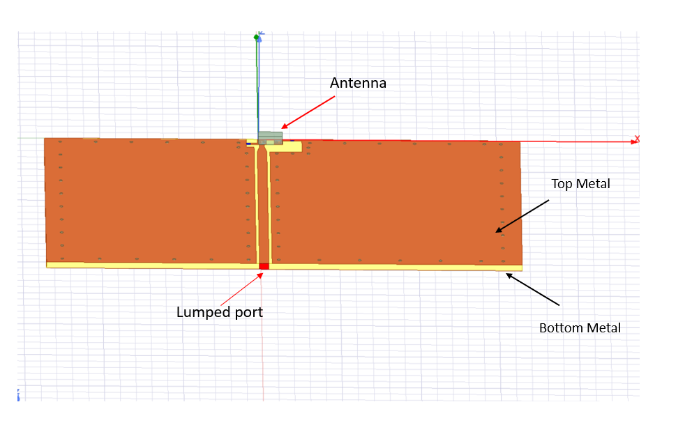
I am trying to simulate an antenna placed on a FR4 substrate (snapshot attached). PCB top and bottom layer are metal connected through VIAs. For this case, to assign a port, I have just drawn a rectangle at the edge of the PCB having a width same as the feedline and length same as the PCB height.
Is it the correct way of assigning lumped port for my case ? If not, would you please tell how should I assign the port accurately?
May 16, 2022 at 7:12 amChinmay Telkikar
Forum Moderator
Kindly do not createduplicateposts. We have answered your question here.
How to provide lumped port for grounded CPW? ÔÇö Ansys Learning Forum
As this is a duplicate post I am closing this.
Thanks Chinmay
Viewing 1 reply thread- The topic ‘HFSS lumped port for grounded CPW’ is closed to new replies.
Innovation Space Trending discussions
 Top Contributors
-
peteroznewman
 5879
5879 -
scabo
 1906
1906 -
Dennis Chen
 1420
1420 -
javat33489
 1306
1306 -
Shyam Prasad V Atri
1021
Top Rated Tags
© 2026 Copyright ANSYS, Inc. All rights reserved.
Ansys does not support the usage of unauthorized Ansys software. Please visit www.ansys.com to obtain an official distribution.
-


The Ansys Learning Forum is a public forum. You are prohibited from providing (i) information that is confidential to You, your employer, or any third party, (ii) Personal Data or individually identifiable health information, (iii) any information that is U.S. Government Classified, Controlled Unclassified Information, International Traffic in Arms Regulators (ITAR) or Export Administration Regulators (EAR) controlled or otherwise have been determined by the United States Government or by a foreign government to require protection against unauthorized disclosure for reasons of national security, or (iv) topics or information restricted by the People's Republic of China data protection and privacy laws.
