Ansys Assistant will be unavailable on the Learning Forum starting January 30. An upgraded version is coming soon. We apologize for any inconvenience and appreciate your patience. Stay tuned for updates.
Electronics

Electronics

Topics related to HFSS, Maxwell, SIwave, Icepak, Electronics Enterprise and more.

Circuit Element (Balun) HFSS Simulation

    • bb2025
      Subscriber

      Hello,

      I'm trying to simulate a balun (abt-8-75-2) in HFSS by importing the .snp information as a circuit element. However, I'm only getting ok results and would like to know if I've set up the balun's geometry correctly in HFSS.

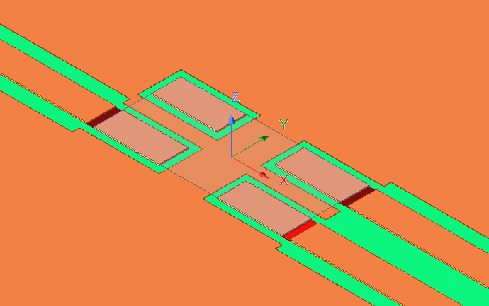
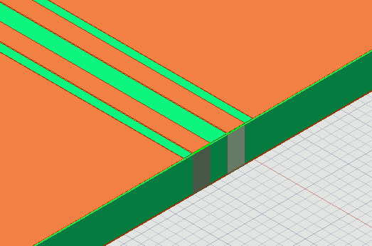
      The pad dimensions are from the manufacturer datasheet and the red squares are lumped ports that are used to import the .s3p file as a circuit element. The results are similar if the remaining pad is tied to ground. A PEC is placed in contact with all the pads to provide a reference.

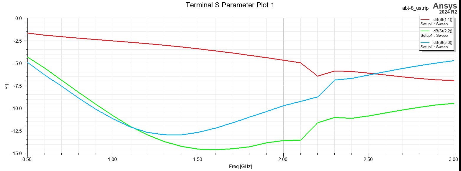
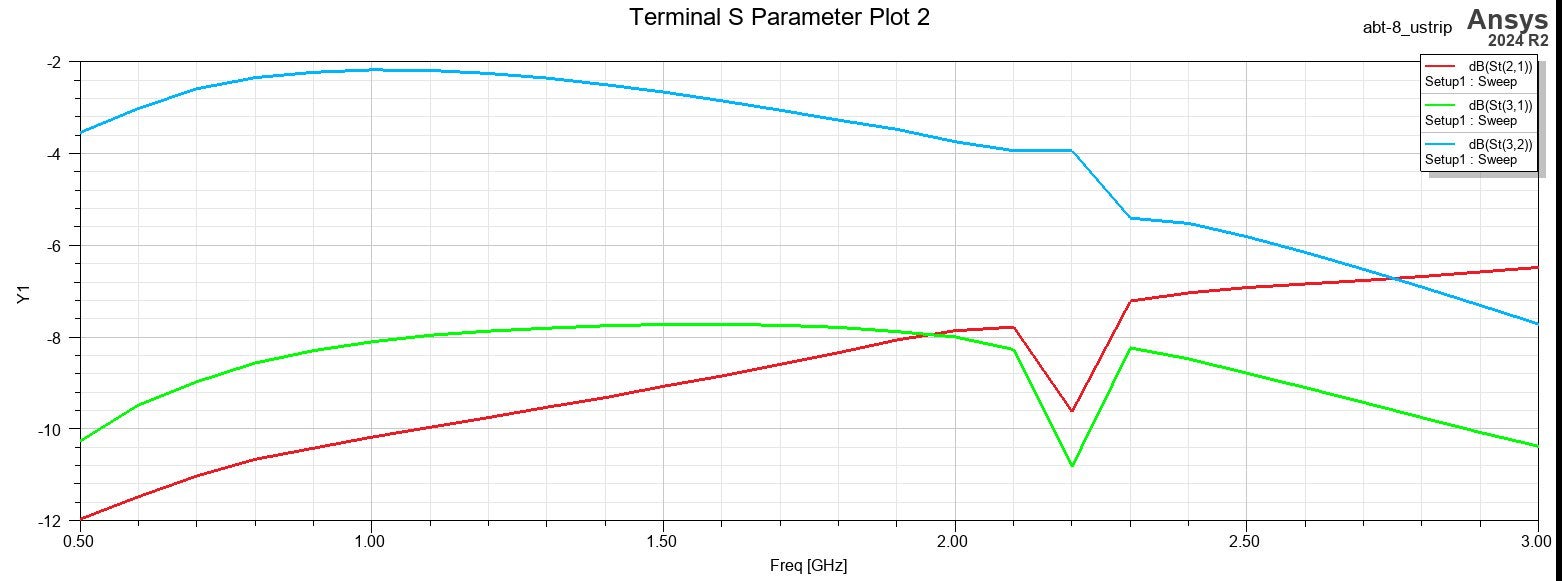
      The ports (lumped ports, 75 Ohm) are shown in the other figure. I am using the terminal solution type. The S_ii and S_ij parameters are shown in the below figures. I realize the device isn't rated for the entire frequency band, but the results aren't good in within band.

      Thanks,

      B.

    • gia.serano
      Ansys Employee

      Can you please highlight the PEC object being used as the reference? - If these traces are connecting to the pads, the ports for the balun should not be series connected in-between the trace and the pads... The ports for the balun should be placed vertically and connected to the reference plane (which could be the ground plane underneath - it is ok to draw the port vertically through the substrate)... 

Viewing 1 reply thread
  • You must be logged in to reply to this topic.
[bingo_chatbox]