To guys who knows about the setting for TSV simulation using HFSS, can you tell me the mistakes about my settings, thanks.
I try to replicate the TSV simulation from: https://core.ac.uk/download/pdf/72787437.pdf
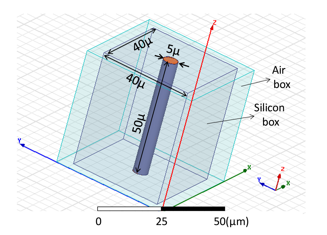
In this paper page15, it shows a 5um-diameter,50um-height, 0.5um-thick SiO2 dielectric, Copper-filled TSV structure surrounded by 40um x 40um x 50 um silicon substrate(10 Siemens/m), whose outer shield is an air box.
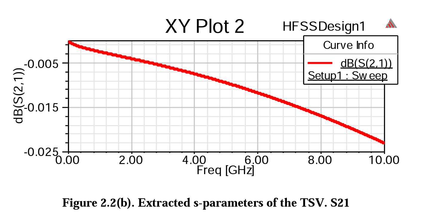
The confused things is about wave port settings. It just says that, " The top and bottom plates of the TSV are selected as wave port terminals to apply the excitations".
I tried many times with different configuration,including: using modal solution with wave port (2 different modes), using terminal solution with terminal wave port, it just cannot get the same S21 picture as it in the paper. sometimes it will have very high insertion loss, some times the simulation just failed with "Solving too low frequency".
Analysis setup: Auto-High Accuracy-Linear Count-0 to 10GHz-501 points.
Hope anyone can answer my question, thank you very much!