-
-
July 4, 2022 at 7:00 am
 Watch & LearnParticipant
In this part we compare the stackups of the printed circuit board between Mentor Xpedition and ANSYS SIwave. The video clearly explains how the different material properties, the thicknesses, and other properties are translated to SIwave. Another important feature shown in the video is the process of generating data files with component values from SIwave. The values are modified and the data file is imported back to SIwave and the component values are changed accordingly to reflect the ones in the bill of materials file. Another key feature shown in the video is using an XML control file that can control the ODB properties to be read in by SIwave and their order. For instance, the file is configured to read in a property field in the ODB++ database that can straightaway translate all component values accurately while importing the ODB++ directory to SIwave.
-


Introducing Ansys Electronics Desktop on Ansys Cloud
The Watch & Learn video article provides an overview of cloud computing from Electronics Desktop and details the product licenses and subscriptions to ANSYS Cloud Service that are...

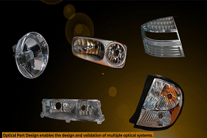
How to Create a Reflector for a Center High-Mounted Stop Lamp (CHMSL)
This video article demonstrates how to create a reflector for a center high-mounted stop lamp. Optical Part design in Ansys SPEOS enables the design and validation of multiple...

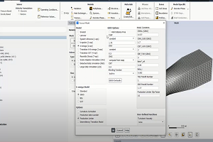
Introducing the GEKO Turbulence Model in Ansys Fluent
The GEKO (GEneralized K-Omega) turbulence model offers a flexible, robust, general-purpose approach to RANS turbulence modeling. Introducing 2 videos: Part 1 provides background information on the model and a...

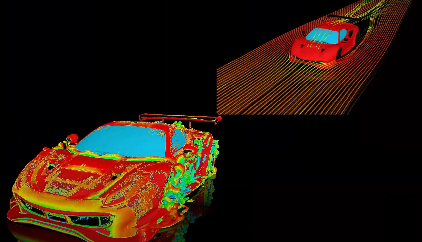
Postprocessing on Ansys EnSight
This video demonstrates exporting data from Fluent in EnSight Case Gold format, and it reviews the basic postprocessing capabilities of EnSight.

- I got “I/O error when reading design” error message when opening an AEDT project with HFSS 3D Layout designs after a system crash. How should I proceed to recover my project?
- ANSYS HFSS: Creating 3D Components
- Error: Extracta view creation failed; extracta run failed: Create process failed with error 2: Could not find application extracta.exe.
- How to Export S-Parameters from HFSS 3D Layout/HFSS 3D Designs ?
- How to Set “Non-Model” Property to an Object in 3D Layout
- ANSYS HFSS: 3D Layout Cut Out Sub-design – Simulation and Post Processing
- ANSYS HFSS: 3D Layout Model from a Cadence Board File
- How to export a design from HFSS 3D Layout to HFSS 3D Classic?
- How to create Output Variables and setup convergence criteria based on output variables in HFSS 3D Layout ?

© 2025 Copyright ANSYS, Inc. All rights reserved.


