Tagged: aggressors, antenna coupling, coupling, electromagnetic interference (EMI), electronics, EMIT, hfss, insertion loss report, pcb, radiated emissions, radio, radio-frequency interference, receivers, return loss report, RF Coexistence, RF Desense, RFI, smartphone, spread spectrum clocks, WiFi receiver
-
-
July 4, 2022 at 7:00 am
 Watch & LearnParticipant
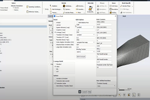
In this video, we run a Desense analysis for the improved design in EMIT. The video also offers a good overview of the EMIT user interface. Two metrics, namely EMI Margin and Desense are utilized in EMIT to identify all possible offenders and eliminate interference completely for this design. A commonly employed frequency modulation technique in electronics design known as Spread Spectrum Clocking is also described and defined in EMIT to significantly reduce electromagnetic interference (EMIT). All contributors of interference occurring within and outside the tuned channel are assessed and eliminated from the modified design of the PCB.
-


Introducing Ansys Electronics Desktop on Ansys Cloud
The Watch & Learn video article provides an overview of cloud computing from Electronics Desktop and details the product licenses and subscriptions to ANSYS Cloud Service that are...

How to Create a Reflector for a Center High-Mounted Stop Lamp (CHMSL)
This video article demonstrates how to create a reflector for a center high-mounted stop lamp. Optical Part design in Ansys SPEOS enables the design and validation of multiple...

Introducing the GEKO Turbulence Model in Ansys Fluent
The GEKO (GEneralized K-Omega) turbulence model offers a flexible, robust, general-purpose approach to RANS turbulence modeling. Introducing 2 videos: Part 1 provides background information on the model and a...

Postprocessing on Ansys EnSight
This video demonstrates exporting data from Fluent in EnSight Case Gold format, and it reviews the basic postprocessing capabilities of EnSight.

- I got “I/O error when reading design” error message when opening an AEDT project with HFSS 3D Layout designs after a system crash. How should I proceed to recover my project?
- ANSYS HFSS: Creating 3D Components
- Error: Extracta view creation failed; extracta run failed: Create process failed with error 2: Could not find application extracta.exe.
- How to Export S-Parameters from HFSS 3D Layout/HFSS 3D Designs ?
- How to Set “Non-Model” Property to an Object in 3D Layout
- ANSYS HFSS: 3D Layout Cut Out Sub-design – Simulation and Post Processing
- ANSYS HFSS: 3D Layout Model from a Cadence Board File
- How to export a design from HFSS 3D Layout to HFSS 3D Classic?
- How to create Output Variables and setup convergence criteria based on output variables in HFSS 3D Layout ?

© 2025 Copyright ANSYS, Inc. All rights reserved.


