TAGGED: photonics
-
-
November 6, 2024 at 1:32 pm
pm796
SubscriberI have a 3D periodic structure, illuminated by a plane wave source (BFAST) at an angle.Â
I have set the source footprint geometry to the same dimension as the periodic region (i.e. same as cross sectional dimension of structure and mesh). Whenever I run the solver, it automatically increases the size of the source geometry, doubling each dimension. See the below screenshot, in which the white outline of the source has been expanded and no longer coincides with the orange line (mesh boundary).Â
Side view for context:
Thanks!
-
November 6, 2024 at 10:36 pm
Kirill
Ansys EmployeeHello pm796,
In short, this is a feature of the GUI. It is implemented to prevent field truncation issues with finite-sized plane wave sources . This topic has been previously discussed on the forum; see Trouble Getting Correct FDTD Plane Wave Region .
Please also check the following resources:Â Broadband Fixed Angle Source Technique (BFAST) and Always extend structures through PML boundary conditions .
Best regards,
Kirill
-
November 7, 2024 at 12:06 pm
pm796
SubscriberÂ
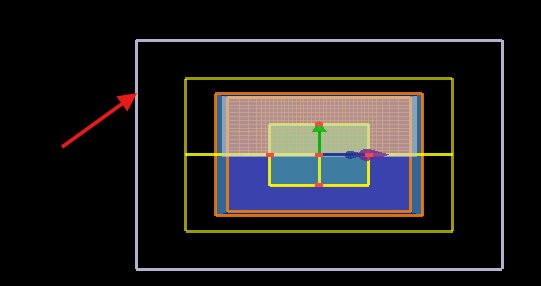
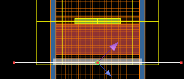
Thank you for your reply, however this does not appear to be explained in the links you give. The BFAST link makes passing reference ‘As usual, the source injection plane should extend completely outside the simulation region..’ as if this was common knowledge, but it doesn't seem to be since others have the same question and I can’t find any information in the ‘reference’ manual.Â
Note I am not trying to use a finite plane wave, I am trying to use an infinite plane wave with an infinitely repeating unit cell (i.e. periodic boundary conditions).
Â
-
November 8, 2024 at 4:18 pm
Kirill
Ansys EmployeeHello pm796,
Thank you for your feedback. I agree that this topic and feature could benefit from better coverage, and we will consider adding more details to our knowledge base.
Generally, any part of the system extending beyond the simulation area should not affect the results. This feature was implemented to help avoid unintentional setup errors.
Please feel free to reach out if you encounter any issues with your simulation results.
Best regards,
Kirill
-
- You must be logged in to reply to this topic.
- Import material .txt file with script
- Errors Running Ring Modulator Example on Cluster
- Absorption cross-section of AuNR excited by prism-based TIR
- How to measure transmission coefficients on a given plane .
- TE Polarization Fraction + Waveguide TE/TM Fraction
- Edge Coupler EME Example Issue
- Lumerical Python API Topology Optimization Error 2025 R1
- 2D inverse design grating coupler
- FDE : Simulation waveguides with electrodes
- Loss of lithium niobate phase modulator
-
2262
-
925
-
599
-
591
-
497
© 2025 Copyright ANSYS, Inc. All rights reserved.