TAGGED: 50-ohms, low-pass-filter, pcb
-
-
March 1, 2024 at 3:33 pm
Nikoloz Sekhniashvili
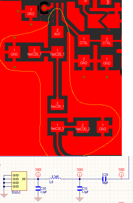
SubscriberI am interested in designing filter circuits, and for this purpose, I have computed the values of lumped components. Nevertheless, I acknowledge that the PCB layout of components also significantly influences performance.
Could you please suggest which Ansys package (HFSS, Nuherz or Siwave) would be suitable for simulating RF PCB circuits, focusing on S parameters and impedance matching?
I would appreciate it if you could also provide some articles related to similar tasks.
-
March 11, 2024 at 4:29 pm
Aymen Mzoughi
Ansys EmployeeFor enhanced accuracy, I recommend using Ansys HFSS in combination with the Modelithics library:
https://www.ansys.com/partner-ecosystem/technology-partners/modelithics
To synthesize impedance matching networks, you can use AEDT Circuit in conjuction with HFSS (Just by drag and drop the HFSS deign into the Circuit design within AEDT).
-
- The topic ‘Simulating the PCB layout for S parameter and impedance matching’ is closed to new replies.


-
5899
-
1906
-
1420
-
1306
-
1021

© 2026 Copyright ANSYS, Inc. All rights reserved.


