

-
-
March 24, 2022 at 12:54 pm
amnonjw
SubscriberHi Lumerical team,
I'm doing simulations of light propagating in photonic crystal waveguide (air holes in a suspended membrane).
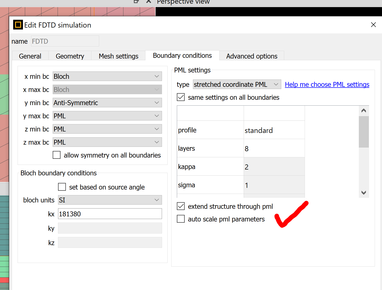
When I downloaded the online example - I noticed that in the boundary conditions tab of the FDTD options, the "extend structure through pml" option is enabled.
This seems to be in contradiction to what I read about in the post here:
March 24, 2022 at 9:47 pmGuilin Sun
Ansys EmployeeThank you for raising this issue. You are right!
As in the page Always extend structures through PML boundary conditions ÔÇô Lumerical Support when the "extend structure through pml" option is enabled it assumes that the structure in front of (adjacent) PML is the same as inside the PML. However for photonic structures it is better not .
Through the years there are many improvements and default setting changes. Although this option has been there for long time, many users may just ignore it, which causes some problems. So later versions evolve
to have ""extend structure through pml" option as default. Coincidently this example was developed after this default change. The example developer might not notice it.
Photonic crystal waveguide is very special, as in real world we would have another regular output waveguide on the right hand side. So your simulation is just a kind of "artificial". It is the PML along the propagation that matters and cause the issue. Depending on your simulation purpose, you may
1: simulate the whole device with regular output waveguide
2: modify the PML to have more absorption for your current settings. The newest version has this feature:
 ÔÇ£auto scale pml parametersÔÇØ.
Please note that due to the Bloch wave nature, the transmission in your current settings will have some change when you change the monitor location, even the PML does not change. This is why #1 is recommended.
March 25, 2022 at 2:10 pmSubscriberHi gsun, thanks for the explanation.
I need to clarify some of the things you wrote:
"1. simulate the whole device with regular output waveguide" - do you suggest to terminate the photonic crystal structure at some x value and continue with a facet or a uniform ridge waveguide?
"2. modify the PML to have more absorption for your current settings. The newest version has this feature - auto scale pml parameters"
I read only yesterday about this new feature in the release notes of ver 2022-R1.1 and I saw your team updated the documentation on the FDTD options.
Do you mean that the PML will perform better over a long periodic structure when "extend structure through pml" option is disabled and "auto scale pml parameters" is enabled (unlik in the above image)?
Does that mean that in a simulation without the new feature I should (theoretically) be able to find some configuration of pml and dt factor (<0.99) for which the simulation would run correctly and without convergence issues?
"due to the Bloch wave nature, the transmission in your current settings will have some change when you change the monitor location, even (though) the PML does not change." (I assume the word "though" was missing in your text").
I assume you refer to the Bloch properties of the theoretical field distributions in general, and not to Bloch boundary conditions of the simulations which I don't use in this simulation.
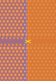
I posted an image of my simulation region without any monitors, so what is the monitor are you talking about?
The goal of my simulation above is to evaluate the fields that are "deep" in the photonic crystal waveguide region that are generated after (b-u-t-t)-coupling to a modes coming from a uniform ridge waveguide. For that I run the simulation with profile monitors at different locations along the waveguide. My goal is to eliminate any reflections from the pml layer so that the fields would represent only the forward propagating waves. Do you think that this is possible after correctly setting the pml layers?
March 25, 2022 at 2:20 pmSubscriberHi gsun, thanks for your answer. Hi have a few things I need to clarify:
"1: simulate the whole device with regular output waveguide"
Do you suggest I should terminate the periodic structure at some x-position and couple the light into a uniform waveguide?
"2: modify the PML to have more absorption for your current settings. The newest version has this feature: auto scale pml parametersÔÇØ.
I read only yesterday about this new feature.
Do you mean that setting "auto scale pml parametersÔÇØ to enabled and setting "extend structure through pml" to disable (unlike in the image above) will allow me to run the simulation correctly with an extension of the structure into the pml layers (like in my image), without convergence issues?
Does that mean that if I use FDTD without the new feature, I need to find (by trials) some configuration of pml layers and dt factor (<0.99) for which I will get a stable simulation?
"due to the Bloch wave nature, the transmission in your current settings will have some change when you change the monitor location, even (though) the PML does not change." (I assume the word "though" is missing in your text)
I didn't show any monitors in my image. What monitor are you referring to?
My goal is to evaluate the distributions of EM fields that are generated deep inside the waveguide due to the light is coupled from the uniform waveguide (on the left). I intend to run the simulation with profile monitors close to the PML region; I assume that with correct PML layers there should be no back propagating waves and so the field distributions will represent the forward propagating modes (my geometry is tuned to have single mode operation at the wavelengths of interest). Are my assumptions correct?
March 25, 2022 at 4:54 pmAnsys Employee"Do you suggest I should terminate the periodic structure at some x-position and couple the light into a uniform waveguide?"
Yes.
"setting "auto scale pml parametersÔÇØ to enabled and setting "extend structure through pml" to disable (unlike in the image above) will allow me to run the simulation correctly with an extension of the structure into the pml layers (like in my image), without convergence issues?"
It is not guaranteed. But you can try.
"Does that mean that if I use FDTD without the new feature, I need to find (by trials) some configuration of pml layers and dt factor (<0.99) for which I will get a stable simulation?"
Yes, most likely you have to modify the PML settings.
"I didn't show any monitors in my image. What monitor are you referring to?"
I believe your ultimate goal is to measure the transmission, not simply to get a converged simulation, even though your current settings have no any monitor except the incident port.
"I assume that with correct PML layers there should be no back propagating waves and so the field distributions will represent the forward propagating modes (my geometry is tuned to have single mode operation at the wavelengths of interest)"
What the mode do you mean here? inside the injection regular waveguide or PhC waveguide? You know inside photonic crystal they are Bloch modes, which means they are volumetric, not planar field distribution. not sure how do you justify it is forward propagating as it has lattice resonance (I called them from my previous research), eg standing waves. How do you know it is single mode? I think this is a more theoretical issue. Even if there is one mode as you expect, if the transmission is close to zero, do you still want it? This paragraph is purely my personal view and suggestions. you can ignore this.
Discrete PML does not absorb 100%. It has discrete numerical errors. IN some case its reflection can be neglected but in other cases it can be significant, even the simulation converges.
Please note that anything changes such as the PhC waveguide length or width, you are simulating different devices in the eye of FDTD.
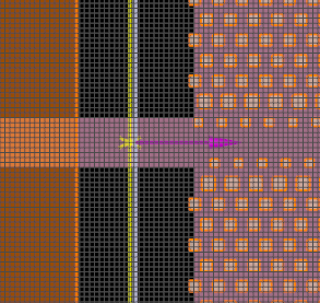
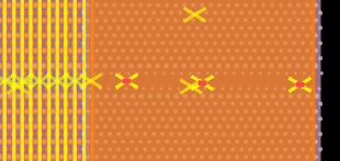
April 3, 2022 at 2:27 pmSubscriberHi When my simulation doesn't converge - I know which PML layer is problematic by replacing it with a metal layer. In the image of my original post - it's the right side (positive x axis). I recently made adjustments to this PML section trying to find the optimal PML configuration with a photonic crystal waveguide:
I reduced dt-factor to 0.65
I increased the number of PML layers
I have a mesh override around circles (holes) of the photonic crystals, but I removed them for the last column before the PML layer.
 The source of radiation comes from uniform waveguide mode. My aim is that inside the photonic crystal waveguide I will have only forward propagating radiation (in the form of a photonic crystal waveguide mode), so I have numerous power monitors (not shown in the pictures) and I evaluate the power along the waveguide. If it's not uniform as function of propagation, then there are back propagating radiation from the PML.
 I have numerous field-time monitors to at different locations to see if there's a build up of power. However when the simulation doesn't converge - the shutoff parameter goes up rapidly but I don't see the power value in any of my monitors goes up. All of my monitors show a power pulse and then decay.
So my next question is: how is the "shutoff level being evaluated? I didn't find any information in the knowledge-base pages and tutorial, other than saying it's evaluating the remaining energy in the system. But if all of my monitors show me that the power is decaying, then where is the energy build-up? Is it inside the PML layers?
(the monitors I position inside the PML don't gather any data)
April 4, 2022 at 1:54 pmAnsys EmployeeIf you tried to use "Metal BC" and it does not diverge, no need to reduce the dt factor.
It is not necessary to use override mesh to evert hole, as it is redundant. Please refer this post: Ansys Insight: About override mesh in FDTD Solutions: its use and settings
I would suggest to use one override region for the whole simulation, which will greatly simplify your settings, and perhaps helpful for the simulation.
Roughly speaking, the shutoff level is a ratio of the residual energy inside the simulation file over the injected energy. In your case, it might indicate that the energy is trapped inside PML.
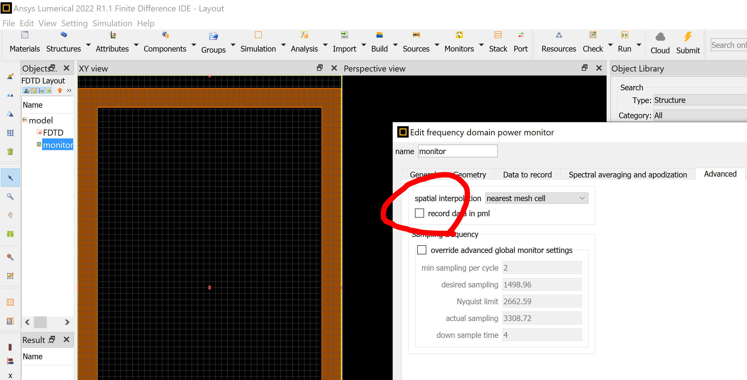
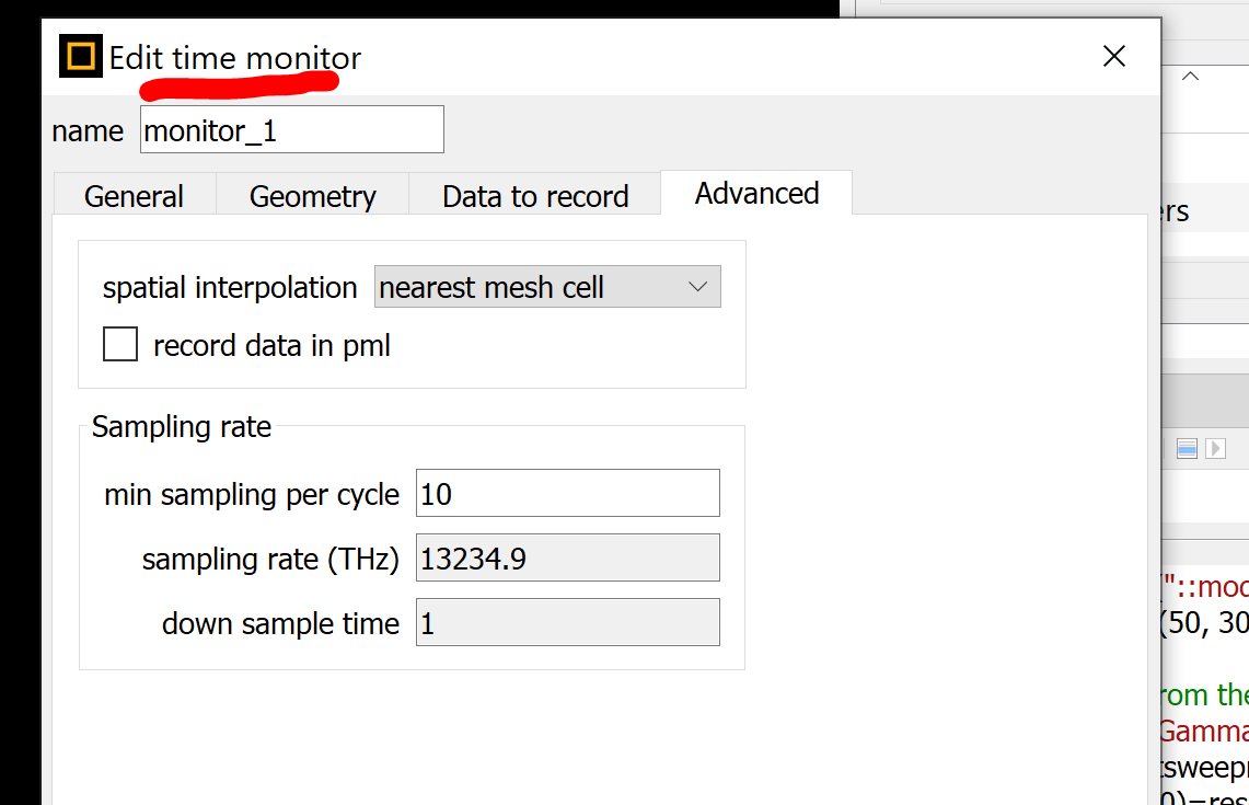
Please enable the monitor to record the data inside PML:
Designing a photonic crystal waveguide without backward scattering can be a very challenge project as the nature of the photonic crystal is scattering in both directions.
April 4, 2022 at 2:07 pmSubscriberHi gsun Thanks for the explanation.
My simulation has numerous override regions around holes as a remnant from another simulation that has a smaller region (like the dimensions of a single super-cell of the PC waveguide) and I want to increase the resolution of the mesh. Above a certain resolution factor it turns that I can reduce the number of samples in total if I use non-uniform meshing for the entire FDTD simulation and place override around holes in my super-cell.
I will check the simulation with a monitor enabled inside the PML, and post the result.
April 4, 2022 at 3:44 pmAnsys EmployeeI still strongly suggest you to use only one override region to simplify the mesh settings. many of them are really redundant, unnecessary. Please try to disable some and check the mesh , and the memory requirement, and see if there some change. Lumerical FDTD uses rectilinear mesh .
April 4, 2022 at 4:47 pmSubscriberI placed several monitors in the PML, 3 of them along the "waveguide core that is in the PML"
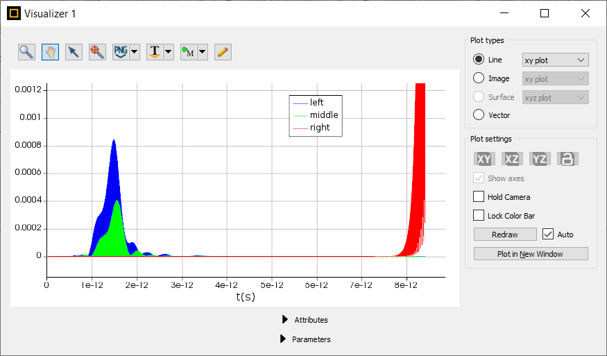
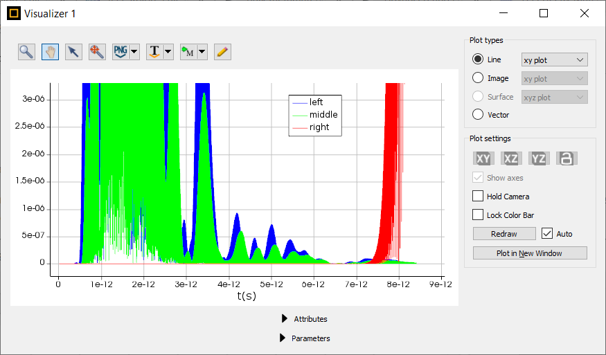
 The power data from these monitors is below. It appears that there's energy build-up at the edge of the PML (the right monitor).
I thought that as the EM radiation propagates along the PML it's absorbed, so when it reaches the edge of the PML it has little energy left. I also expected to see a weak pulse in the right monitor that appears around time moments 2ps
April 5, 2022 at 7:07 pmAnsys Employee"I thought that as the EM radiation propagates along the PML it's absorbed, so when it reaches the edge of the PML it has little energy left. I also expected to see a weak pulse in the right monitor that appears around time moments 2ps
"In any case, it looks to me like even though shutoff condition isn't reached - the problem of energy diverging is confined to PML only, so the data collected within the DTDT region within the simulation time is valid. Is that a correct assumption?"
This will depend on when the simulation terminates: if it terminates before the "burst of power" returns to the simulation region, the monitors inside simulation can give reasonably accurate results. However, since light travels fast, usually the problematic "burst of power" will enter into the simulation region and the results in monitors will not be reliable. That said, you could terminate the simulation around 7e-12 seconds where autoshutoff level is low. This is only valid based on the information you provided. Please check if any other time monitors can have low signal strength around this simulation time.
Viewing 10 reply threads- The topic ‘Simulating Photonic Crystal waveguide – Boundary conditions and satbility’ is closed to new replies.
Innovation Space Trending discussions
 Top Contributors
-
peteroznewman
 6455
6455 -
scabo
 1906
1906 -
Dennis Chen
 1457
1457 -
javat33489
 1308
1308 -
Shyam Prasad V Atri
1022
Top Rated Tags
© 2026 Copyright ANSYS, Inc. All rights reserved.
Ansys does not support the usage of unauthorized Ansys software. Please visit www.ansys.com to obtain an official distribution.
-


The Ansys Learning Forum is a public forum. You are prohibited from providing (i) information that is confidential to You, your employer, or any third party, (ii) Personal Data or individually identifiable health information, (iii) any information that is U.S. Government Classified, Controlled Unclassified Information, International Traffic in Arms Regulators (ITAR) or Export Administration Regulators (EAR) controlled or otherwise have been determined by the United States Government or by a foreign government to require protection against unauthorized disclosure for reasons of national security, or (iv) topics or information restricted by the People's Republic of China data protection and privacy laws.
