-
-
August 20, 2024 at 8:01 am
johnny_hsiao
Subscriberhttps://optics.ansys.com/hc/en-us/articles/360041780494-Defect-on-a-metal-surface
1)_The illumination in this article is assumed to be a focused spot rather than illumination over a specific area. Are there any other articles that use standard image calculation with illumination over a specific area?
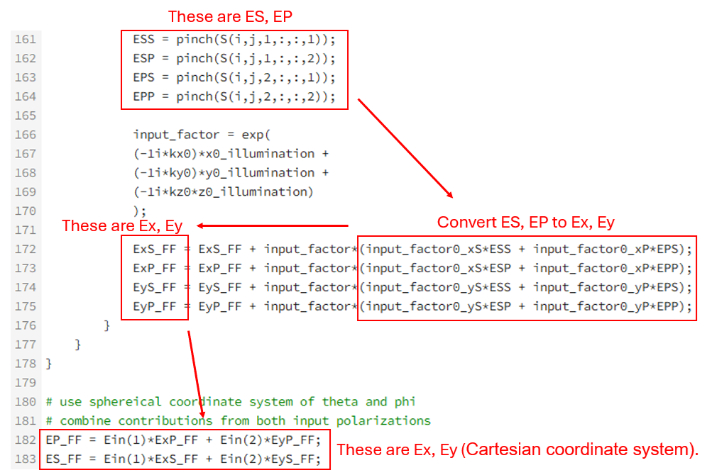
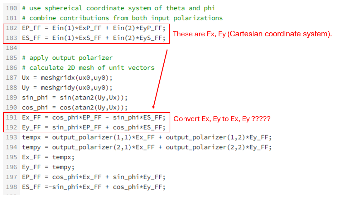
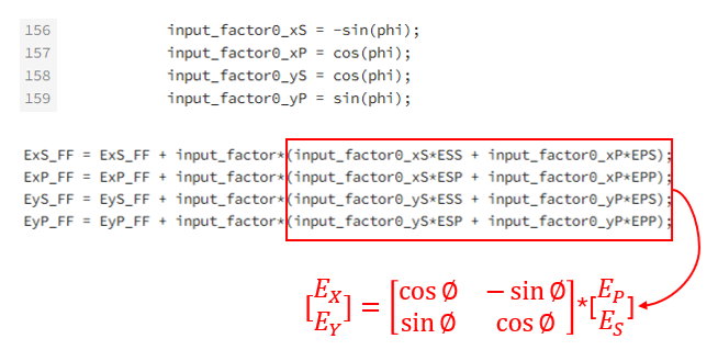
2)_The EP, ES and Ex,Ey transformation confused me. Please see the description below.
Why is the transformation matrix multiplied again in line 191 & 192.
-
August 20, 2024 at 3:55 pm
Guilin Sun
Ansys EmployeeThis example uses plane wave and periodic-type BCs so it is for periodic structure. If you want to simulate non-periodic structure you can use Gaussian beam.
For the script, Lines 172~175 are not Ex,Ey. The subscripts xy are meant for incident xy polarization.
-
August 21, 2024 at 2:46 am
johnny_hsiao
Subscriber1)_I would like to use the S matrix calculation method to simulate defects. I referred to another topic "Optical-Defect-Metrology-S-Matrix", but that optical imaging is mainly based on a scanning spot. So I am trying to modify it to a standard image calculation method, and researching how to write the script and looking for related articles.
2)_If lines 172~175 are not Ex,Ey. What is the input_factor0_(xS, xP, yS, yP) mean? I thought that is transform matrix between Es, Ep and Ex, Ey.
-
August 21, 2024 at 9:37 pm
Guilin Sun
Ansys EmployeeMaybe you can visit the original example to get clear understanding: https://optics.ansys.com/hc/en-us/articles/360041768554-Optical-Defect-Metrology-S-Matrix
The first transformation is for input filter, and the second one is for output filter.
-
- You must be logged in to reply to this topic.


-
3467
-
1057
-
1051
-
929
-
896

© 2025 Copyright ANSYS, Inc. All rights reserved.


