-
-
March 30, 2026 at 6:06 pm
smaturi
SubscriberHello,
I am seeking technical assistance regarding a persistent UI behavior in Ansys Electronics Desktop 2025 R1.3 specifically within the HFSS SBR+ solution type.Issue Description: I am currently working with a simulation where the SBR+ Solution Setup is correctly configured for a Single Point at 28 GHz. However, the Layered Impedance Boundary dialog does not appear to retain user-defined frequency inputs. Even after manually entering 28 GHz and clicking Calculate to update the Real and Imaginary impedance values, the "Test Frequency" field reverts to the default 1 GHz as soon as the dialog is closed and reopened.
Technical Details:
- Software Version: Ansys Electronics Desktop 2025 R1.3
- Solution Type: HFSS SBR+
- Setup Configuration: Solution Setup is confirmed at 28 GHz
- Observation: While the dialog note states that impedance will be calculated using the Solution Frequency during the solve, the inability to verify the 28 GHz calculation within the boundary properties UI makes it difficult to confirm the accuracy of the material assignment properties prior to running the simulation.
Could you please advise if there is a specific method to ensure the 28 GHz setting is permanently retained within the boundary properties UI, or if this is a known display-only behavior?
Thank you for your time and assistance.


-
March 31, 2026 at 12:40 am
Takeshi Itadani
Ansys Employee
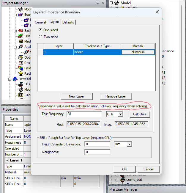
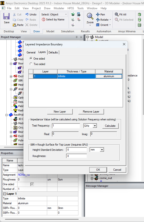
The Impedance Value in the Layered Impedance boundary condition is purely a calculator function. While 1GHz is selected by default, this doesn't mean only the calculated value at this frequency is applied. This function is simply for pre-checking the applicable surface impedance.ÂIn actual analysis, the surface impedance at the Solution Frequency or Frequency Sweep frequency is calculated and applied during the analysis.ÂMore importantly, there are some corrections needed in the Layered Impedance boundary condition settings.You've selected "One sided" in the Layers settings, but this is used when applying a thin film material to the surface of a 3D solid. The correct setting is to set the Thickness of the base 3D solid object to Infinite, and then input the desired thickness for the thin film material to be applied using the Layered Impedance boundary condition.ÂLooking at the image settings, there's only one Layer, and the Thickness is set to Infinite, which is an incorrect use of the Layered Impedance boundary condition. Are you trying to set material properties for a 2D sheet?If it's a layer, you need to select Two-sided, not One-sided.Also, although aluminum is selected as the material, if you only want to set one conductor on the 2D sheet, please consider using Finite Conductivity boundary conditions instead of Layered Impedance boundary conditions.Even with Finite Conductivity boundary conditions, when setting on a 2D sheet, please set it as Two-sided. -
April 1, 2026 at 4:31 am
smaturi
SubscriberDear Takeshi,
Thank you very much for the detailed explanation and the technical corrections regarding my setup. To clarify my design intent, I am modeling a laptop surface as a 2D sheet using aluminum.
I have been implementing your suggestions and have the following observations to share:
Group Assignment Error: I attempted to apply the Finite Conductivity boundary to the device model. However, because the laptop is an assembly of individual components (keypad, ports, chassis), I received a system error: "FiniteCond1 can not be assigned on entity of type Group". It appears this boundary cannot be applied to a collection of entities simultaneously.
Layered Impedance Implementation: As an alternative, I successfully updated the Layered Impedance boundary to "Two sided". I also replaced the "Infinite" thickness with a specific value of 1µm using aluminum.
Material Constraints: Given that my model is a complex assembly containing various materials like Plastic (ABS), is it more appropriate to continue using Layered Impedance on the specific conductive surfaces rather than Finite Conductivity?
I now understand that the 1 GHz display is purely a calculator function and the solver will correctly use the Solution Frequency during analysis.
Thank you for your time and assistance.
-
April 2, 2026 at 12:32 am
Takeshi Itadani
Ansys Employee> Layered Impedance Implementation: As an alternative, I successfully updated the Layered Impedance boundary to "Two sided". I also replaced the "Infinite" thickness with a specific value of 1µm using aluminum.ÂAs mentioned above, Two-sided is a method for setting boundary conditions on 2D sheets. This is fine if all the objects to which you are trying to apply boundary conditions are 2D sheets.Â> Material Constraints: Given that my model is a complex assembly containing various materials like Plastic (ABS), is it more appropriate to continue using Layered Impedance on the specific conductive surfaces rather than Finite Conductivity?ÂFinite Conductivity boundary condition can only impose the material properties of a single conductor. If you want to impose other material properties as boundary conditions, please use the Layered Impedance boundary condition.
-
- You must be logged in to reply to this topic.
-
5834
-
1906
-
1420
-
1305
-
1021
© 2026 Copyright ANSYS, Inc. All rights reserved.