-
-
February 8, 2023 at 10:33 am
Philip Collins
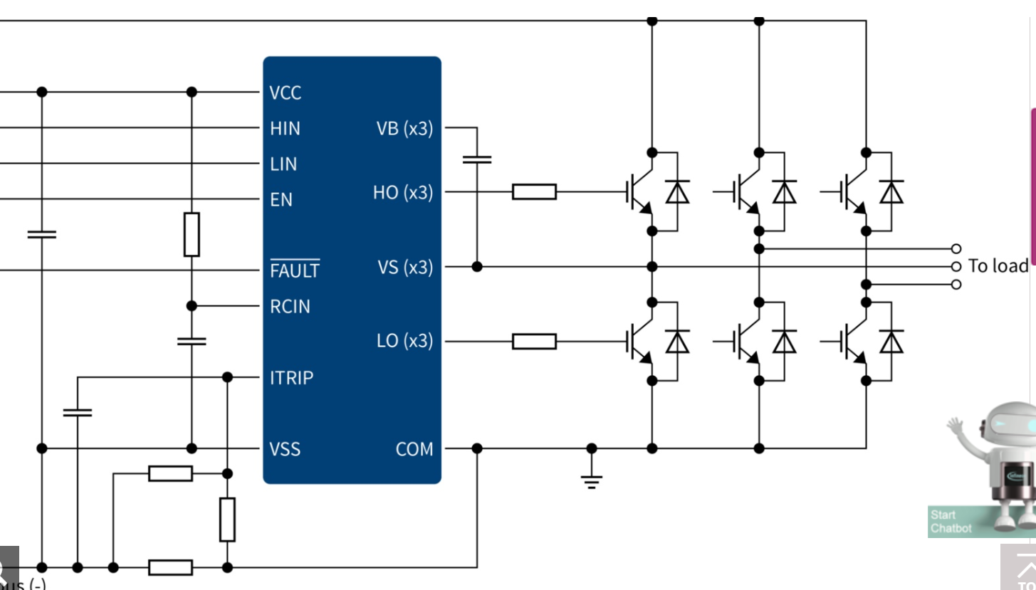
SubscriberHello. I'm going to model a PCB layout for a three-phase inverter circuit. It's a high current design and I'm mostly interested in simulating the DCIR drop in SIwave then doing the thermal analysis in Icepak. As a complete beginner, I have watched a few of the tutorials but I'm still struggling with the best way to represent the MOSFETs. See the attached generic picture of a similar circuit.
I know I can designate a given power dissipation for each MOSFET in Icepak. But to model the effect of the PCB trace geometry I need a good representation of the DC current in the bridge section. What is the best method? Should I add a current source to each MOSFET drain terminal and a voltage source to each MOSFET source terminal?
If anyone has done a similar analysis I would be very grateful for some tips.
Many thanks
Phil
-
February 14, 2023 at 3:26 pm
Philip Collins
Subscriberbumping this. are any Ansys people able to direct me to some resources?
-
March 27, 2023 at 11:57 am
Praneeth
Forum ModeratorHi Philip,
Thank you for reaching out and your patience is much appreciated.
Please let us know if you want to model a MOSFET with a circuit approximation or design actual 3D geometry in Icepak. If it is about circuit approximation then Ansys personnel may not be of good help. Will leave it to other experts in the forum to guide you better.
Best regards,
Praneeth.
-
- The topic ‘Modelling MOSFET in SIwave/Icepak for PCB simulation’ is closed to new replies.


- HFSS Incident Plane Wave excitement mode
- Simulation of capacitor combining eddy currents with displacement currents
- How to calculate eddy and hysteresis losses of the core?
- Ansys Maxwell 3D – eddy current
- How to determine initial position in motion setup
- dq graph non-conformity
- Simplorer+Maxwell Cosimulation results and Maxwell results mismatch
- Parametrizing coil “terminals” with coil geometry
- On-chip inductor design
- Maxwell circuit – PWM

-
1406
-
599
-
591
-
550
-
366

© 2025 Copyright ANSYS, Inc. All rights reserved.


