We have an exciting announcement about badges coming in May 2025. Until then, we will temporarily stop issuing new badges for course completions and certifications. However, all completions will be recorded and fulfilled after May 2025.
Electronics

Electronics

Topics related to HFSS, Maxwell, SIwave, Icepak, Electronics Enterprise and more.

How to set simulation conditions for coplanar microstrip line CPS (or differenti

    • vicastle
      Subscriber

      Hello! I encountered some problems when simulating and designing coplanar strip lines (or differential lines) using HFSS, please help: 

      1. I can run the official example differential_microstrip.aedt normally, but when I removed the metal boundary condition at the bottom of the air box and replaced it with a radiation boundary condition (removed GND), I ran again and encountered an error: Solving adaptive frequency ..., process hf3d error: Too few conductors were found on port 1.  There should be one conductor for each terminal, with one additional reference conductor.  Unintentional contact between conductors may cause this error.. Please contact Ansys technical support. Must this GND exist? Can I set one of the coplanar strip lines as the signal line and the other the GND, like a coplanar waveguide (CPW)? Additionally, Deembed seems to have a significant impact on the results. What does this variable mean?

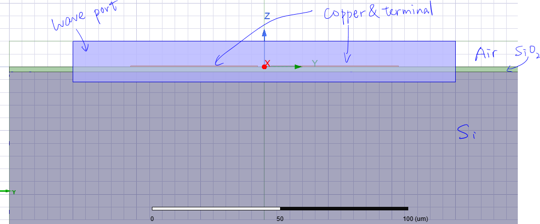
      2. My ultimate goal is to design a pair of ground-signal (GS) electrodes (sub millimeter level) on the chip with a frequency range of around 0-20GHz. The substrate of the chip is silicon (hundred um level) and silicon dioxide (um level), as shown in the schematic diagram below. Therefore, there are electrodes and two substrates within the range of microwave wavelengths. How should I set waveport and terminal to obtain the correct results? Should the size be set to about ten times the electrode width or spacing, as in CPW, or should it be set to near the wavelength level?

    • kirthika
      Subscriber

      Hi

      I did a similar simulation recently. 

      Assign a modal waveport with one conductor as signal and referencing to the other conductor as ground on both sides.

      The port would be 5`10 times the height of the substrate in Z direction and in the Y direction, 5~10*(width + gap).

      Once you run the simulation, you will be able to see the excitation mode under port field display. and it should look as below. 

      So the port size will vary with varying substrate height, CPW width and gap.


    • kirthika
      Subscriber

      Also, refer this guide from HFSS for defining port. /courses/wp-content/uploads/sites/2/2021/07/HFSS_GS_2020R2_EN_LE6_Port_Basics.pdf

    • dushyant.marathe
      Ansys Employee

      Thanks Kirthika for answering some of the queries on Waveport.

      There was another query about de-embedding.

      Deembedding in HFSS refers to the process of adding or subtracting a transmission line to modify the S-parameters at the ports. This technique is used in situations where you want to shift the reference plane of the S-matrix for any port by adding or subtracting a length of lossless transmission line. In HFSS, deembedding is allowed only for wave ports and Floquet ports. I would suggest refereing HFSS help PDF for more information.

    • geff
      Subscriber

      Hello, I have a similar challenge. Trying to design the coplanar stripline on GaAs substrate of thickness 500um.  What port size should I use? 

    • kirthika
      Subscriber

      I tried the port size I recommended above. It did not correlate with a published work and another software. 

      I used 5 to 10 times the height of the substrate 100um and the port was too narrow for very thin line widths.

      Could you recommend the port size for a substrate of 100um and 500um?

      Coplanar lines of width 4um and 2um spacing.

Viewing 5 reply threads
  • The topic ‘How to set simulation conditions for coplanar microstrip line CPS (or differenti’ is closed to new replies.