
-
-
July 21, 2021 at 8:25 am
warrensu
SubscriberThis was asked in the reply section of another question but it didn't receive an answer so I'm posting a new one.
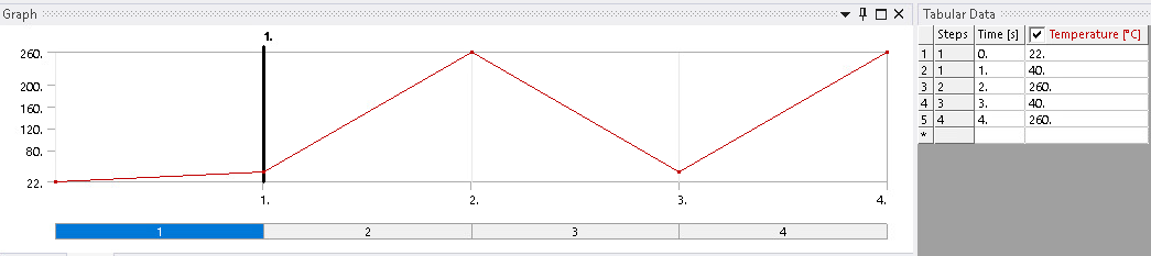
I like to model a thermal cycling/reflow situation where my PCB will heat -> cooldown -> reheat again. In reality, deformation after three cycles will definitely be different from after just one cycle of heating and cooling. In ANSYS Static Structural, I added the following temperature points to my thermal condition.
July 29, 2021 at 3:51 pmdlooman
Ansys EmployeeTo get a different solution you need to have a property that produces nonrecoverable strain such as plasticity or creep. It might also be possible to model the reflow condition with the "Birth and Death" feature by "killing" the solder material at high temperature.
Viewing 1 reply thread- The topic ‘How to realistically model PCB warpage?’ is closed to new replies.
Innovation Space Trending discussions
 Top Contributors
-
peteroznewman
 5809
5809 -
scabo
 1906
1906 -
Dennis Chen
 1420
1420 -
javat33489
 1305
1305 -
Shyam Prasad V Atri
1021
Top Rated Tags
© 2026 Copyright ANSYS, Inc. All rights reserved.
Ansys does not support the usage of unauthorized Ansys software. Please visit www.ansys.com to obtain an official distribution.
-


The Ansys Learning Forum is a public forum. You are prohibited from providing (i) information that is confidential to You, your employer, or any third party, (ii) Personal Data or individually identifiable health information, (iii) any information that is U.S. Government Classified, Controlled Unclassified Information, International Traffic in Arms Regulators (ITAR) or Export Administration Regulators (EAR) controlled or otherwise have been determined by the United States Government or by a foreign government to require protection against unauthorized disclosure for reasons of national security, or (iv) topics or information restricted by the People's Republic of China data protection and privacy laws.
