TAGGED: -waveguide, coupling, lumerical, taper, wrong-modes
-
-
November 21, 2024 at 10:18 am
taynara.deoliveira
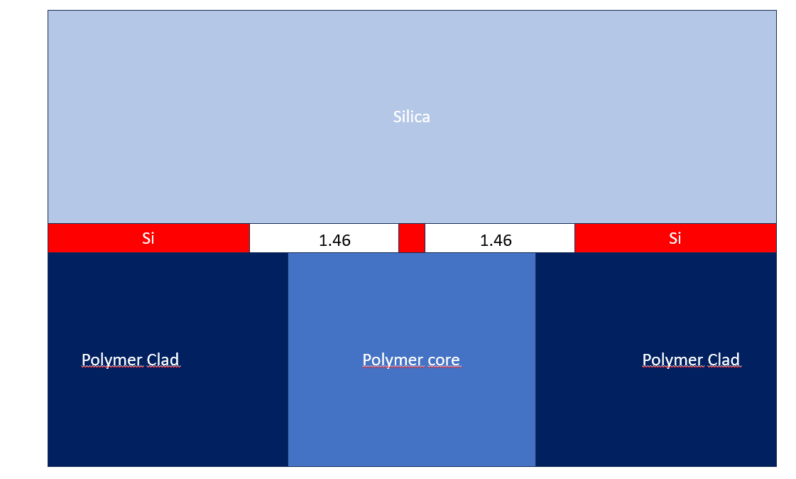
SubscriberWhen simulating adiabatic coupling between SOI taper and polymer, considering the following structure:
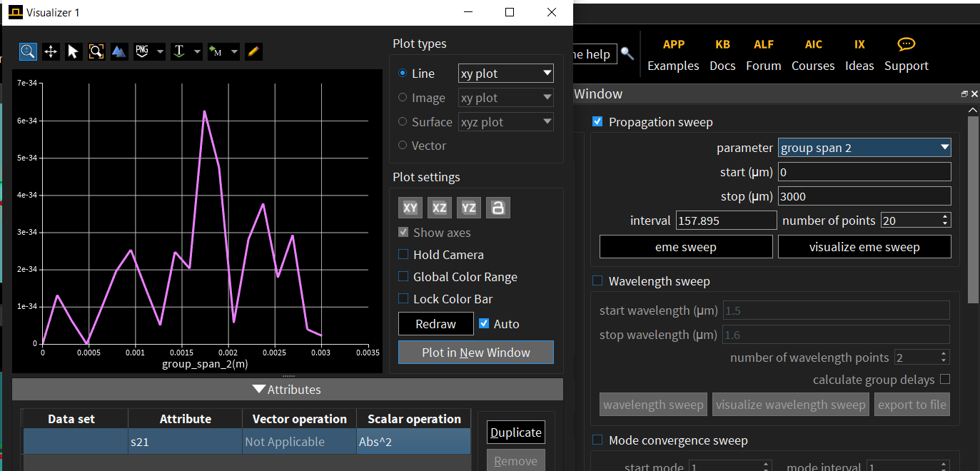
The EME solver finds, of course, slab modes. The fundamental mode of the waveguide, which is the taper, in the middle, can be only found as the 15th mode. Even if I select this 15th mode, which is the one I am interested, when doing the propagation sweep, the adiabatictly coupling is near to zero. No light couples to the polymer.
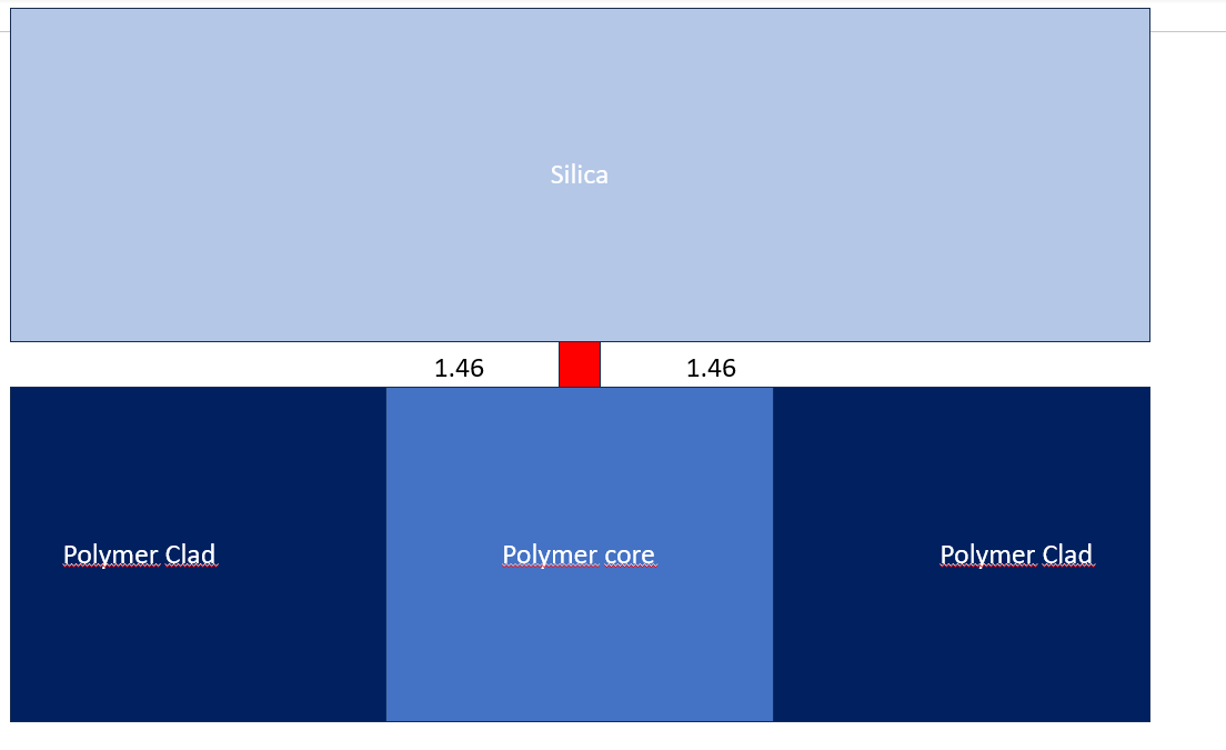
When then I remove the Si slab, and simulate the strucuture:
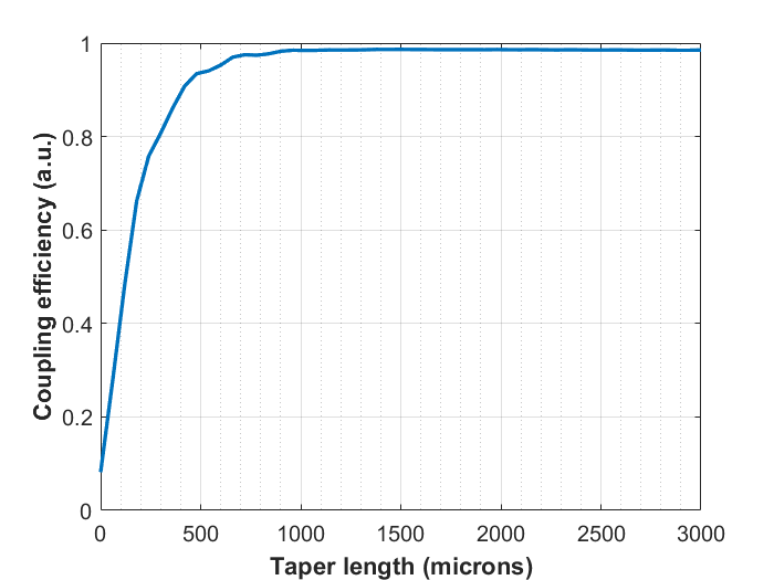
Then I get this nice result:
Of course, the mode 1 in the previous strucuture is the fundamental mode of the taper waveguide, and the other modes are cladding modes and etc.
I don't understand why I can't achieve any coupling in the first structure, even when I select the desired mode that, in reality, will be the mode we intend to excite in the waveguide. Is it because this mode is the 15th one and not the Mode 1?Would be nice to have some help on that.Thank you.Taynara -
November 22, 2024 at 9:04 am
Afroditi Petropoulou
Ansys EmployeeDear Taynara,
Thank you for contacting us.
The way to select the mode of interest is to go to the excitation port and select the mode from the list. I guess this is what you already did.
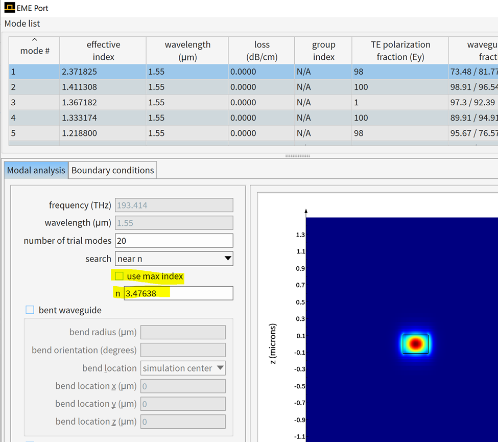
Alternatively, you can deselect the “use max index” option and enter in the n box a value that is close to the effective index of the mode:
But both approaches will result in the same mode selection. They don’t eliminate the fact that when having the side Si waveguides, other modes are supported, and light can couple to these modes more efficiently than in the polymer mode. The coupling between modes can be calculated using overlap - Script command – Ansys Optics.
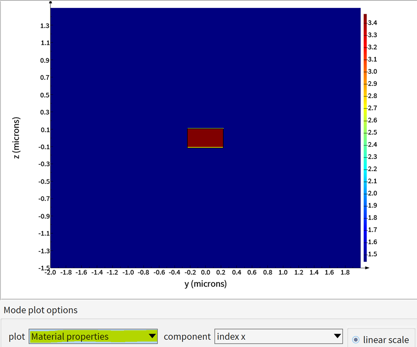
In any case, could you share with me more information regarding the structure that you have used (refractive index of each material, wavelength of interest, dimensions of the structures, port dimensions and boundary conditions (metal or PML)) or even a screenshot from the port mode calculation window showing the material properties as in the following picture?
Best regards,
Afroditi
-
November 22, 2024 at 10:48 am
taynara.deoliveira
SubscriberThanks for the reply.
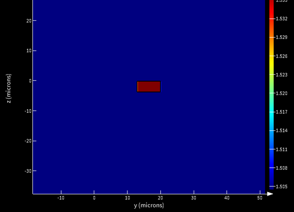
The polymer RI: 1.537 (height x width = 3x7um)
The polymer cladding RI: 1.5045(throught the BC)
Si: from database (0.3um x 0.5um), taper length is 10um
Silica: 1.45 or 1.444 (throught the BC)
BC: Metal (but I tried with PML already)
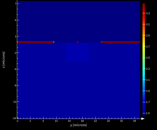
I understand that the mode will couple more to the silicon. However, the slabs are away from the polymer, as you can see in the image, meaning they are not touching the polymer. So, the mode guided in the middle waveguide will couple to the polymer because it has the highest refractive index in that configuration. Do you agree? The slabs are 7um away from the taper tip.
Indeed, I already tried the options you mentioned, but the coupling is still zero, even when I select the correct mode (or mode of interest).
Silicon side
Polymer side:
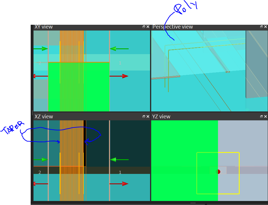
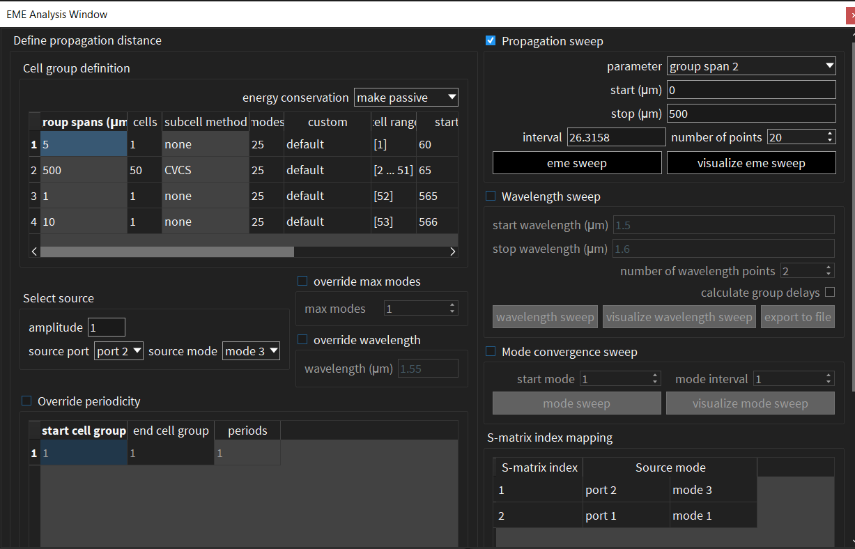
EME setup:
Maybe, something is wrong in the way I am calculating the s-matrix? or the Si slab should be even more distant than 7um?
Thank you.
-
November 22, 2024 at 1:36 pm
Afroditi Petropoulou
Ansys EmployeeDear Taynara,
I don’t understand exactly the geometry used. The excitation side is:

and the output port is:
Is this correct? In the last photo where is the top silica, polymer, polymer cladding and side Si slabs? Why are the y and z spans different?
Another option that can affect the result is the number of modes in each cell. If you choose a mode that is not one of the first modes, you must ensure that this mode (the one that is really close to this one as the structure gradually changes) will be also found in the rest of the cells. To ensure that, you can either use many modes in the cells which will increase the simulation time, or use custom modes for each group:
Best regards,
Afroditi
-
November 28, 2024 at 3:41 pm
taynara.deoliveira
SubscriberHi,
It is correct. The strucure group is rotated.
I think is indeed related to the mesh. I will try what you suggested
But now i am facing another problem. I don't know why i often receive this error: Meshing complete in 0.093750 seconds of CPU time
Error: Port mode set for port '::model::EME::Ports::port_1' could not be found or updated.It says that the port could not be updated, And the Port is there... I changed from left to right, but i suppose this is allowed and should not be a problem. And the autoupdates is selected
Do you know what it can be?
Thank you.
-
November 29, 2024 at 11:25 am
Afroditi Petropoulou
Ansys EmployeeDear Taynara,
What did you change and got this error? Was it only moving port1 from left to right? Was there a specific reason for this change? It shouldn’t give an error though. Can you share some screenshots of the ports’ and EME settings as well as the selected modes in each port?
Best,
Afroditi
-
- You must be logged in to reply to this topic.


-
3492
-
1057
-
1051
-
965
-
942

© 2025 Copyright ANSYS, Inc. All rights reserved.

