We have an exciting announcement about badges coming in May 2025. Until then, we will temporarily stop issuing new badges for course completions and certifications. However, all completions will be recorded and fulfilled after May 2025.
Photonics

Photonics

Topics related to Lumerical and more.

FDTD far-field projection error

TAGGED: 

    • minki99
      Subscriber

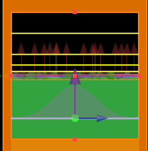
      I'm working in to simulate the far-field scattering pattern of 10x10um substrate with ultra-transparent(T~0.92) thin film(~100nm). 

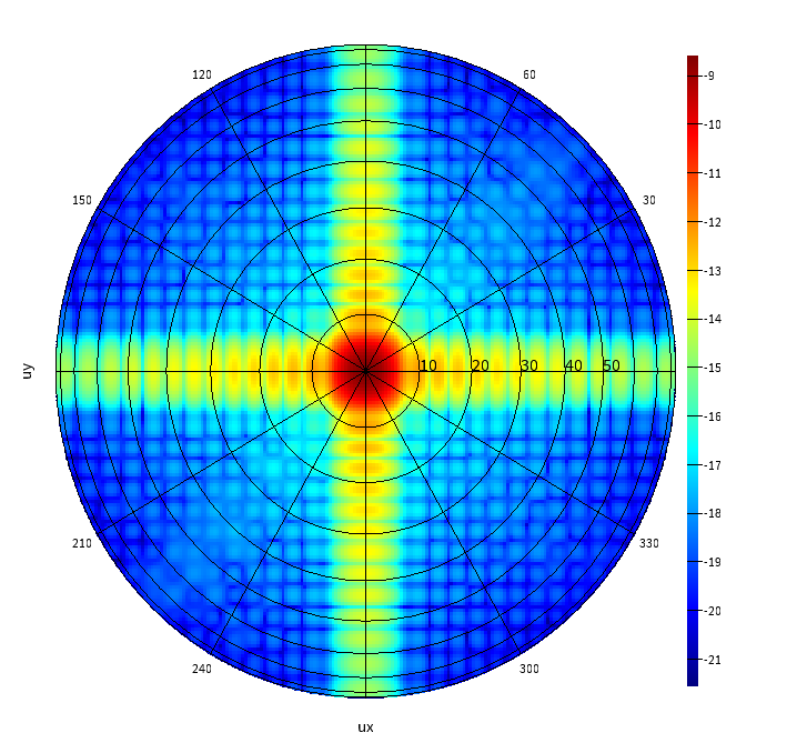
      When I using the far-field projections property of DFT monitor, there are some awkward Moire pattern is appeared.

      I'm not sure exactly what causes the above pattern to appear. I have tried changing the monitor's position and the mesh size, but it was of little use. The attached photo shows the result observed with a monitor placed 0.5 µm away from the film surface using a 10 nm mesh.

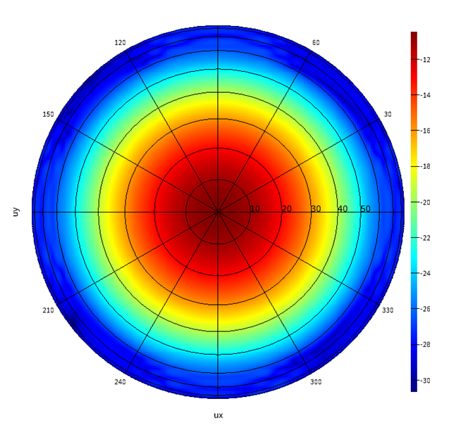
      The only way to suppress this pattern was by reducing the Gaussian beam waist from 3 µm to 1 µm (right side of image). Could you please explain exactly what causes this pattern and advise on how to resolve it?

      Sincerely.


    • Guilin Sun
      Ansys Employee

      It seems there are two issues:

      1: the field at the monitor edge is not zero. You will need to increase the xy span of the simulation and monitor.

      2: the sinc^2 like ripples are mainly due to #1, which you may improve it by use of the Gaussian farfield filter.  However it is "improve". the best way is to significantly increase xy spans.

      btw: what are the arrows at the top? are they local Gaussian beams? it seems there are many nano structures. Due to diffraction, light spreads widely and they are coherently interfere. Please increase xy spans.  

Viewing 1 reply thread
  • You must be logged in to reply to this topic.