Hello,
Eye Diagram:
While you are setting up your Driver/Receivers within the Siwizard in Siwave, you need to make sure to all nets have something assigned to it. If you have extra nets, you may need to remove the unnecessary ports on the nets you are not interested in (this will make sure only the nets you are interested in show up in Siwizard). Typically, in those types of errors messages, it tells you exact what nets needs to be assigned an IBIS model. Double check and make sure that you have a driver/receiver assigned to that net. Exposing/unexposing nets only exposes the pin on the s-parameter model when it is created/used in Circuit. It does not hide/remove the pin from being solved.
Also, make sure that everything that is set as a "Receiver" as the
Type assigned to it, then is has an appropriate "Driver" on the other side. For example, if you have a list of nets that start at U1 and then ends at J1 (and all the nets at the J1 side is set to "Receiver" type), then make sure that those same nets at the U1 side is set as a driver.
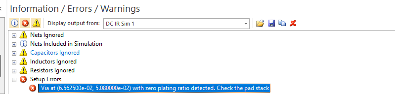
DCIR Drop Test Issue:
Sometimes the Siwave does not exactly show you the exact location of the via placement. Is there any vias around that has zero-plating defined within it's padstack properties? Siwave not showing the exact location of the via might be a defect of the tool, but it is hard to confirm without having the project.
Here are my suggestions:
- First, try to identify if that one particular via is important to the simulation. Cross reference is with you PCB board in another ECAD viewer. Since the simulation finishes, it may not be a big deal if it is not relevant to the area you are checking for DCIR.
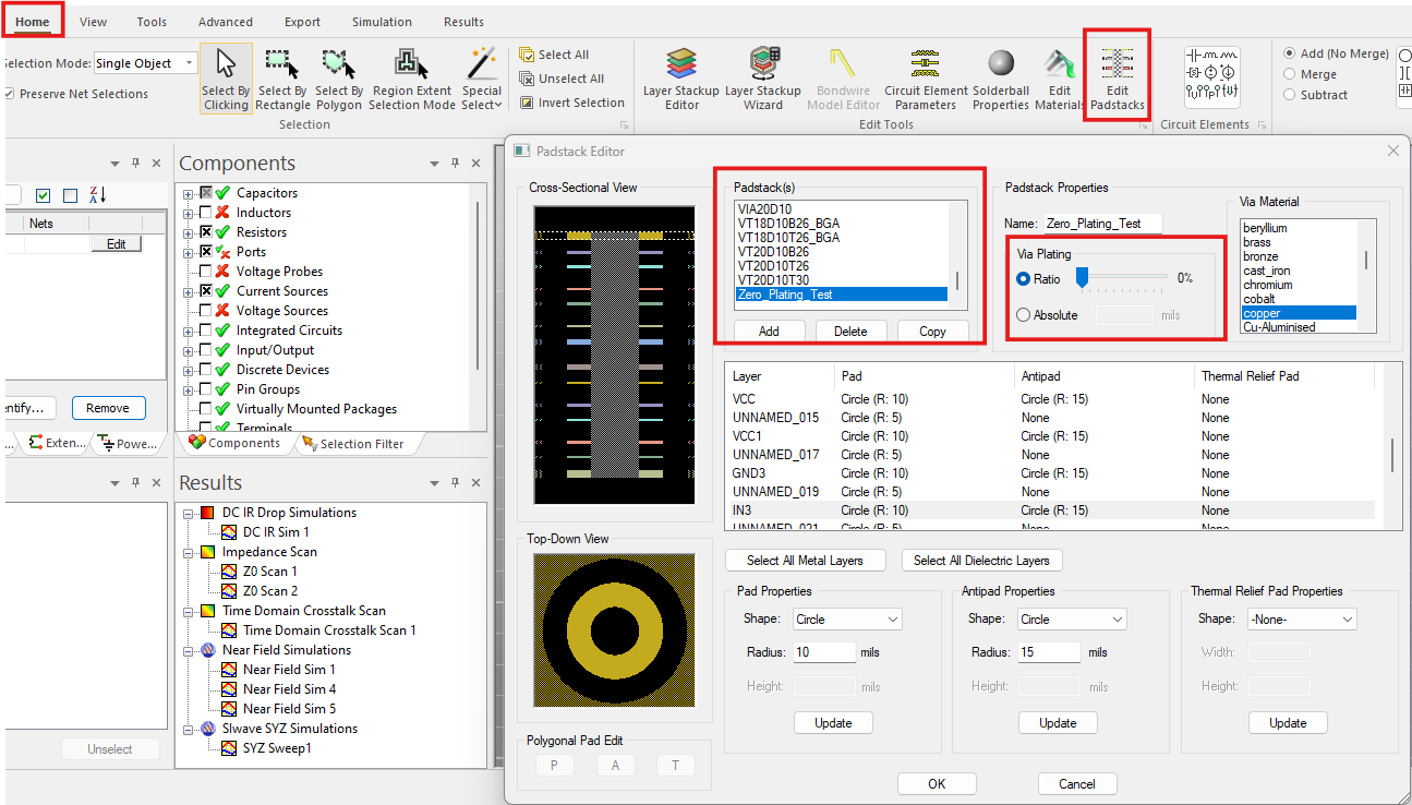
- Secondly, Verify that all your padstack definitions are correctly defined for you vias. You can check padstacks by doing to the "Home" tab and then select the "Edit Padstacks" button. This will open up the padstacks and you will need to go through each padstack to find out which one has zero-plating define and change it. See image below
Regards,
Ansys Technical Support