-
-
October 17, 2023 at 5:01 am
Nishita RVCE
SubscriberHello ANSYS community,
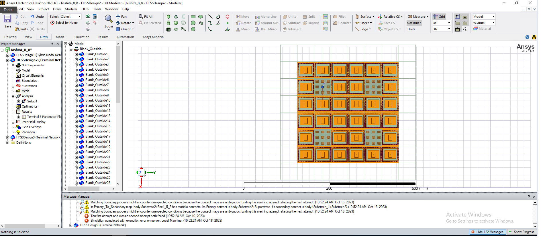
I am encountering an issue with my HFSS simulation while working on an S and X band array antenna design. I've been trying to resolve this problem for some time but haven't had much success, so I'm reaching out to the community for guidance.
Error Description: The error message I'm encountering is [Tau first attempt and classic second attempt both failed]. This error occurs during the simulation process, and I'm struggling to identify the root cause and solution.
Problem Details:
- I have thoroughly checked my geometry and ensured it's accurate.
- Meshing has been optimized and verified.
- Excitation, boundary conditions, and materials are correctly defined.
- HFSS version- 2023 R1 license
I would greatly appreciate any guidance, tips, or solutions from the ANSYS community. If you've encountered a similar error in your work or have expertise in antenna design, please share your insights. Your help would be invaluable in overcoming this roadblock.
-
October 19, 2023 at 1:55 am
Faezeh Tork Ladani
Ansys EmployeeHi Nishita,
There is mesh issues. It is likely related to the way the array is set up.
I see you are inserting several instances of the same component. In finite array, we insert only one instance of the component and then create an array. Check this open example: From file>Open Examples..>HFSS>Antennas>FiniteArray_Radome_77GHz_3D_CADDM. The example comes with a short document. It should help setting up.
Also, before creating the whole array, run the two components separately with proper boundary condition (as isolated elements) and make sure they would run fine with no mesh issues.
-
- The topic ‘Error in HFSS for S and X Band Array Antenna Design – Need Help!’ is closed to new replies.


-
6379
-
1906
-
1457
-
1308
-
1022

© 2026 Copyright ANSYS, Inc. All rights reserved.


