-
-
October 29, 2024 at 11:57 pmRuzan SokhoyanSubscriber
Hello,
Â
I have a question regarding simulating electro-optic modulators. I am trying to simulate a modulator, as shown in the schematic below. In my simulation, LNO and Si are defined as semiconductors while SiO2 is defined as a dielectric. I use two gold contacts on the side. I set the potential of one of the contacts to zero while the voltage applied to the second contact is being swept from 0 V to 5 V. I record the electric field in the LNO. As seen in the image below, the spatial distribution of the absolute value of the electric field in the LNO appears asymmetric. This does not make much sense to me. Where do you think this could be coming from?
Â
-
October 30, 2024 at 8:19 pmGuilin SunAnsys Employee
I am not sure what kind of symmetry you expect: between two contacts? it is less likely, since the potential is gradually reduced to drive the current. Please test this example and see if the static field is symmetric: https://optics.ansys.com/hc/en-us/articles/360042327854-PIN-Mach-Zehnder-modulator
You may check result at zero voltage and compare it with higher voltage.Â
Â
-
October 31, 2024 at 10:48 pmRuzan SokhoyanSubscriber
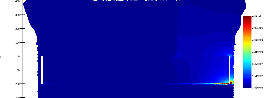
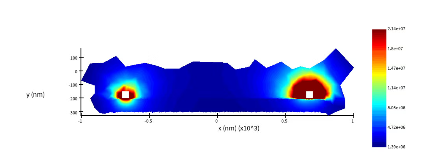
One example of a symmetric distribution of the electric field can be found in this paper.
https://www.nature.com/articles/s41467-020-14539-y
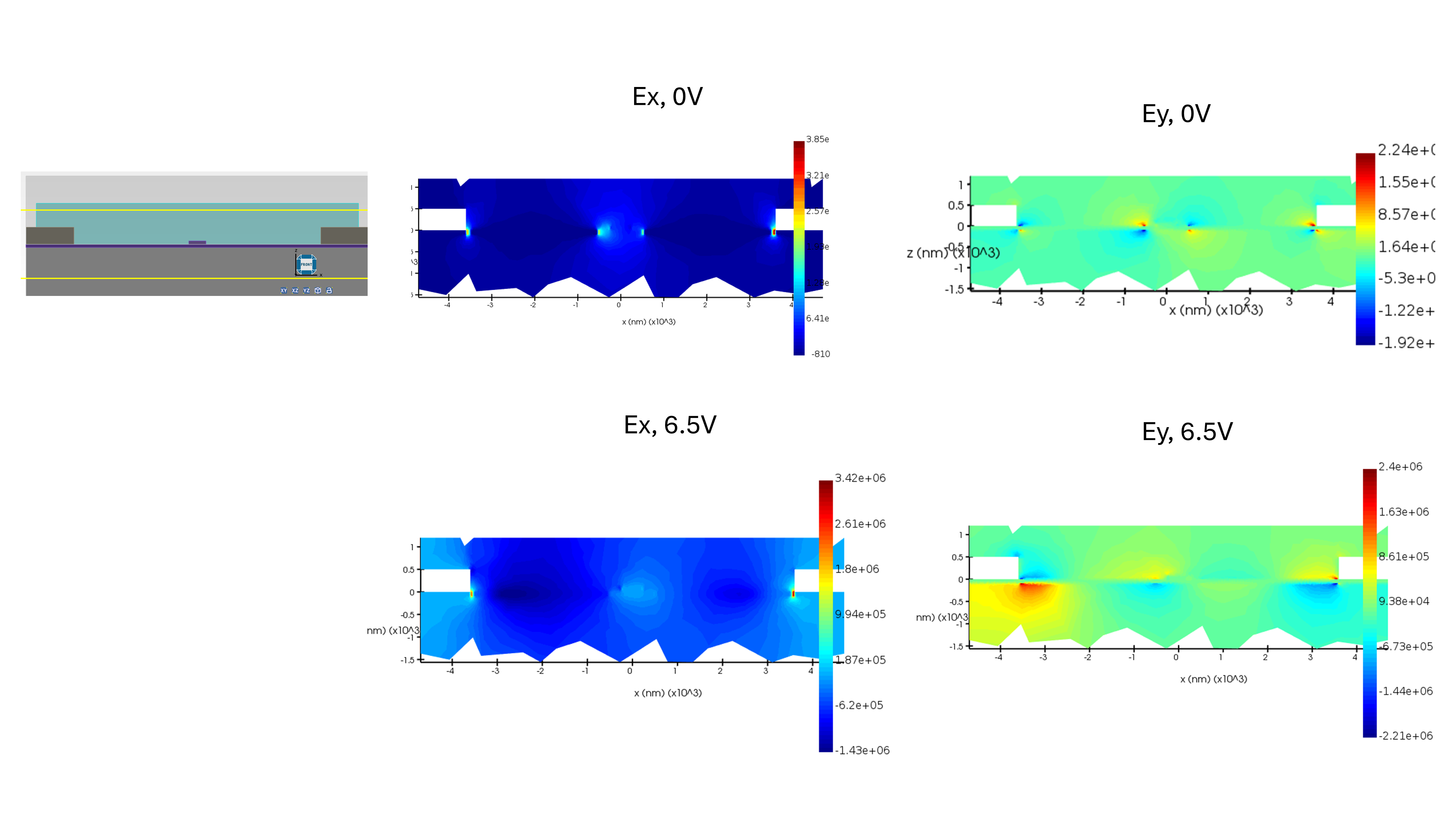
 The paper's image can be seen below. The paper considers a situation when two gold electrodes are placed on a lithium niobate substrate. As you see from the image below, the distribution of the absolute value of the electric field is symmetric with respect to x.
Â
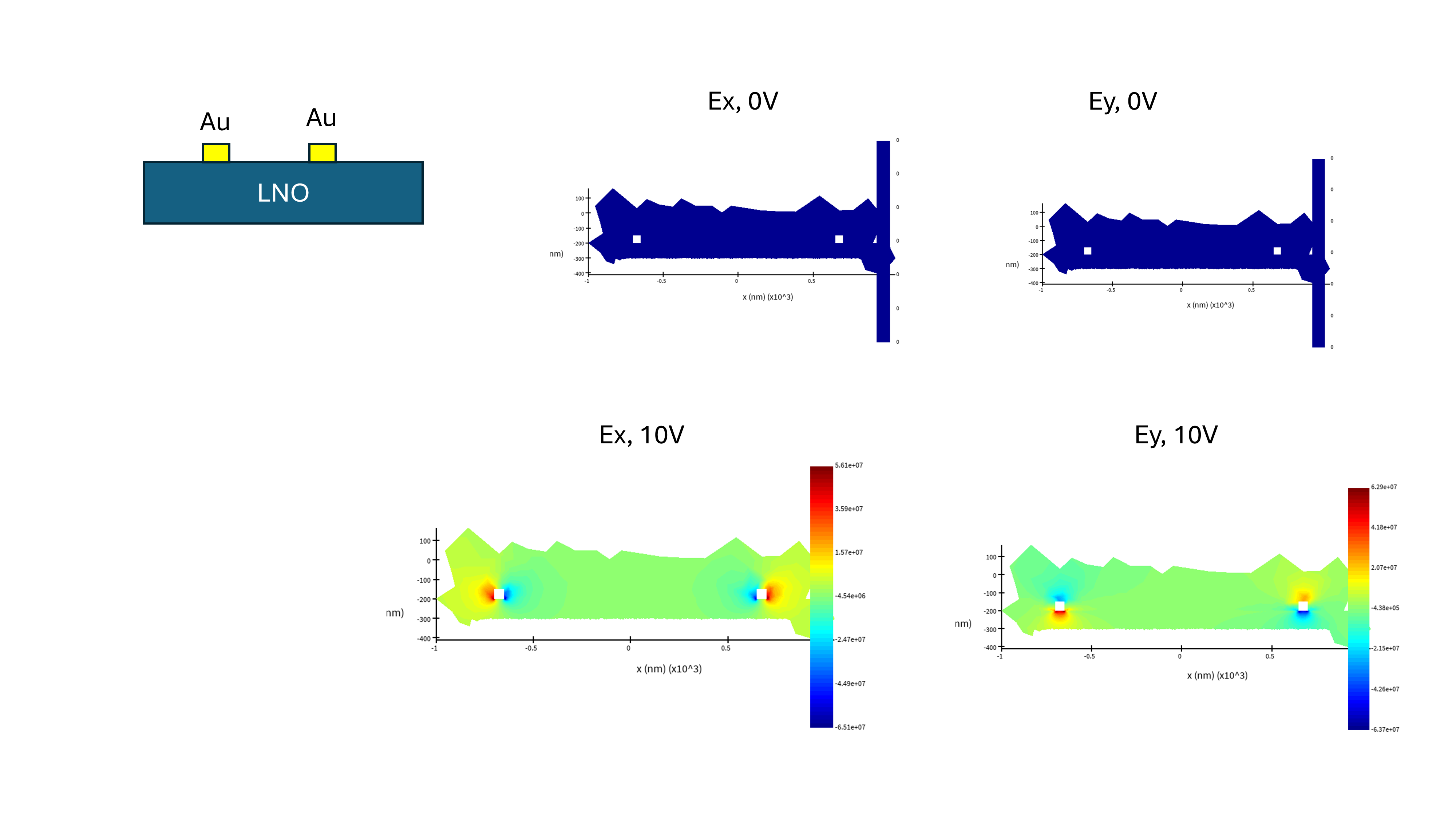
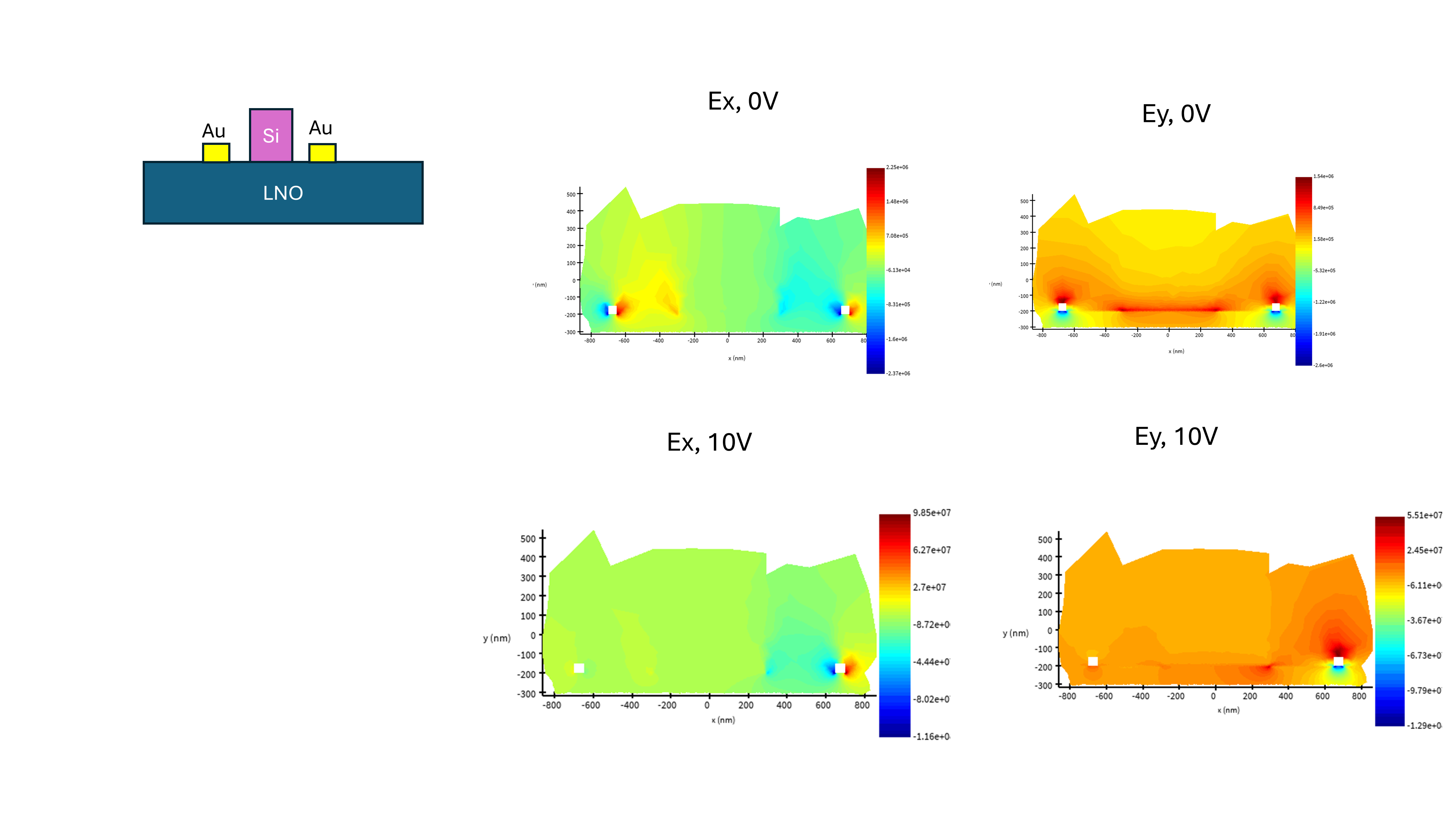
However, in my simulation, I obtain an asymmetric distribution of the electric field. Why would that be the case?
To clarify, in my simulation, lithium niobate is modeled as a semiconductor.
Â
-
October 31, 2024 at 10:53 pmRuzan SokhoyanSubscriber
Regarding the example you mentioned https://optics.ansys.com/hc/en-us/articles/360042327854-PIN-Mach-Zehnder-modulator, if I run the file, the electric field distribution is symmetric.Â
Â
However, if I model the silicon pad under the electrodes as a dielectric with the same DC permittivity, the electric field becomes asymmetric
Why is that the case?
-
October 31, 2024 at 10:58 pm
-
October 31, 2024 at 11:02 pm
-
November 6, 2024 at 1:01 amRuzan SokhoyanSubscriber
Hi Guilin,
Thank you for your help. I actually found a mistake in my original simulation featuring Au electrodes on the lithium niobate substrate. In my original simulation, the gold electordes were 1 nm above the LNO. I fixed the mistake and the simulation results are shown below. It looks like the simulation results are aligned with the literature reports for geometries featuring au gold electrodes on LNO. But when I introduce a Si brick between the electrodes and place it on LNO, I observe strong asymmetry. This result does not seem to be aligned with similar results in the literature (for example, see figure 2 of this paper https://www.mdpi.com/2304-6732/11/10/987). In my simulation, both LNO and Si are modelled as semiconductors. What do you think is wrong with my simulation setup?
-
November 6, 2024 at 2:10 amRuzan SokhoyanSubscriber
Regarding the example of the Mach Zender interferometer, I indeed see the slight asymmetry in the electric field distribution at 0 V and 6.5 V. Do you think this asymmetry is physical or a result of the numerical error? As seen above, this asymmetry becomes very dramatic when the silicon pad is replaced with a dielectric material with the same DC permittivity. Why is there such a dramatic difference between results observed in the two simulation setups?
Â
Â
Â
-
November 6, 2024 at 4:25 pmGuilin SunAnsys Employee
I think it is the physics, as E=-gradient(V), and due to charge distribution the gradient is not a constant. As you can see, some places have strongger electric fields.
-
November 6, 2024 at 5:05 pmRuzan SokhoyanSubscriber
Thanks for the comment. However, for me is still unclear why replacing the semiconducting material with an insulator of the same DC permittivity as the semiconductor yields drastically different results. Shoudn't results be identical if no current flows through the system?
-
November 6, 2024 at 5:13 pmGuilin SunAnsys Employee
The two materials have totally different material properties. Even at the zero voltage, semiconductor has charges but insulator does not have any, and actually is not invovled in meshing.
-
- You must be logged in to reply to this topic.
- Difference between answers in version 2024 and 2017 lumerical mode solution
- Errors Running Ring Modulator Example on Cluster
- INTERCONNECT – No results unless rerun simulation until it gives any
- Import material .txt file with script
- Trapezoidal ring
- Help for qINTERCONNECT
- Issues with getting result from interconnent analysis script
- Absorption cross-section of AuNR excited by prism-based TIR
- How to measure transmission coefficients on a given plane .
- Topology Optimization Error
-
1406
-
599
-
591
-
550
-
366
© 2025 Copyright ANSYS, Inc. All rights reserved.