-
-
July 17, 2023 at 5:45 am
micali
SubscriberDear all,
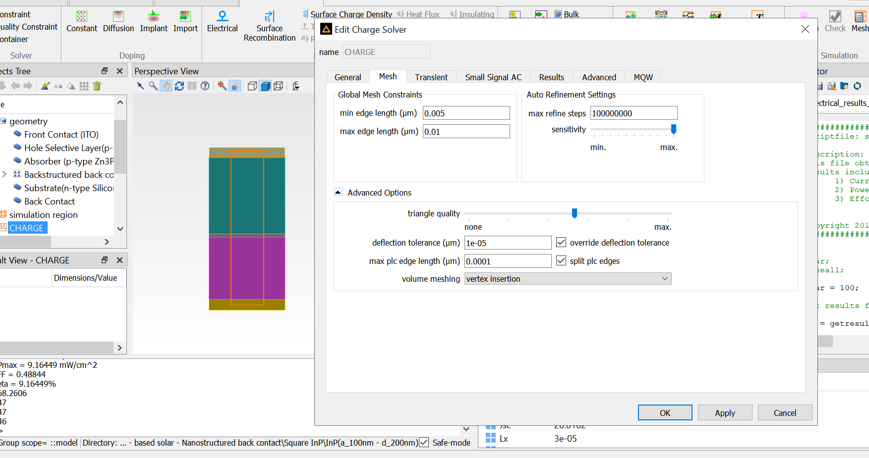
I'm trying to run my simulation with these mesh parameters (attached picture). The problem is that this strucure has:
1- thin layer (10 nm )
2- different dopoing region
3- a complex optical generation rate profile that sometimes gives me the error (optical generation constraint)
The simulation has some issue to reproduce the exact doping profile and generation rate. I tryed different combination of paramters and these only works for simulation region with a width smaller than 150 nm. In this case my simulation need to be at least 300 nm but it doesn't converge at all and fail after generation the mesh.
Does anyone have some tips?
-
July 25, 2023 at 4:32 pm
Guilin Sun
Ansys EmployeeThis is common. Please refer to this article: Troubleshooting convergence errors in CHARGE – Ansys Optics
Please consider the following suggestions in addtion to the article:
1: using local mesh constraint for the thin layer
2: using larger min and max edge lengths in general
3: reduce the sensitivity
4: in advanced options, increase the max plc edge length except the thin layer is thinner than 10nm.
5: increase the iteration limits.
6: please check if any material used has large bandgap, which can lead to huge difficulty for concerging.
Please also refer to
Quality mesh constraint (Finite element) - Simulation object – Ansys Optics
Mesh constraint (Finite element) - Simulation object – Ansys Optics
Lastly, please write post in Photonics forum later: Photonics (ansys.com)
-
July 27, 2023 at 8:19 am
micali
SubscriberThanks for the reply.
So concerning your suggestions:
- The simulation region already has a mesh constraint for the thin layer of 10 nm, but I don't know why it's not enough to define the doping region well. The transition for the doping of that layer falls in the 10 nm layer leading to a distorted and no-sense band alignment. For a very complicated mesh that defines better the doping region the simulation diverges. Do you have any suggestions to sufficiently define the doping with the mesh?
- If I reduce the sensitivity or the iteration limit the mesh constraint is ignored by the software
Thanks in advance
-
July 28, 2023 at 8:43 pm
Guilin Sun
Ansys EmployeePlease refers to this article: Troubleshooting convergence errors in CHARGE
Diverging in CHARGE is complicated. You may need to further modify the contstraints and the number of iteration.
I am not sure I understand the last item. reducing sensitivity will refine the mesh. Maybe you can stick at high sensitivity.
SENSITIVITY: This setting controls the threshold at which the mesh will be refined due to the gradient in the doping density or optical generation rate. The default value will roughly correspond to a limit of a factor of 2 change in the doping density or generation rate over the span of an element in the mesh.
Is this simulation at 0 v? if not, please reduce the voltage step, and initial voltage if it is not zero.
-
- The topic ‘Divergent simulation for large simulation region’ is closed to new replies.


-
3407
-
1057
-
1051
-
896
-
887

© 2025 Copyright ANSYS, Inc. All rights reserved.


