-
-
February 17, 2024 at 5:29 pm
Samad Atta
SubscriberHello community,
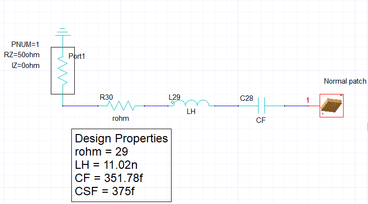
So i have done my Q-matching to enhance a model of my probe-fed patch antenna and i have this:
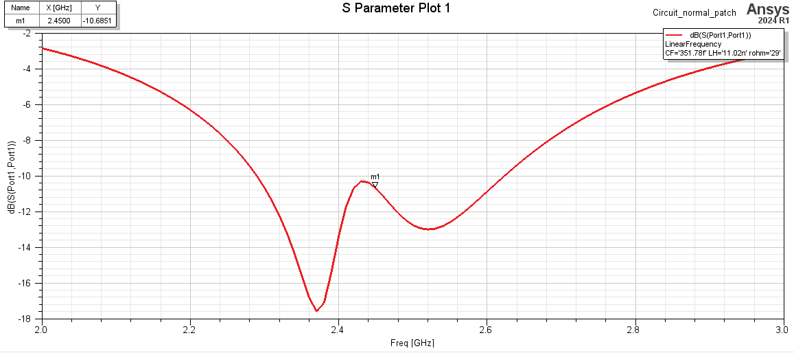
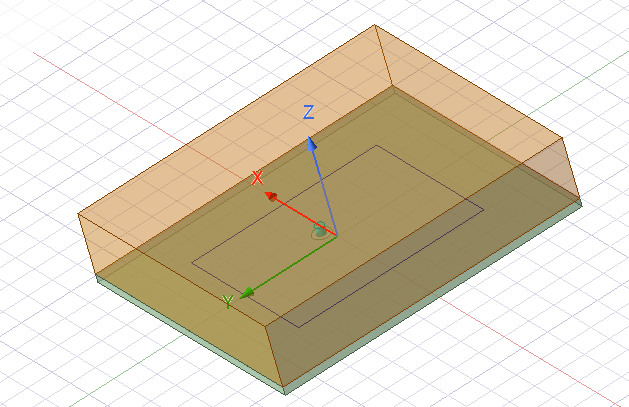
mind you the patch antenna being matched is:
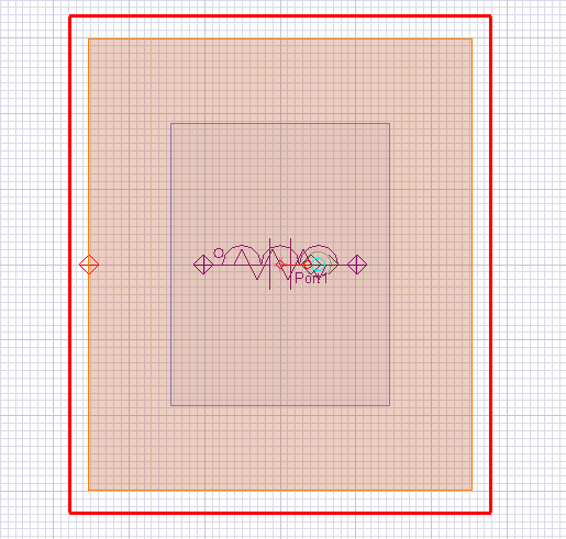
Â
A bottom view is:
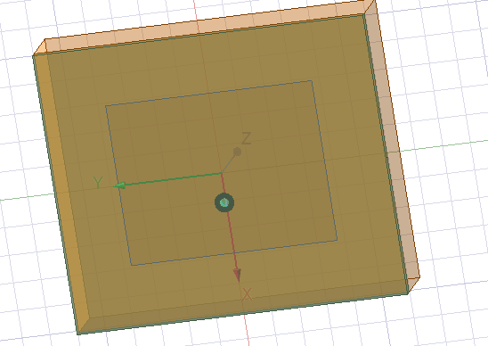
Where the ring you see at the bottom is the lumped port I defined for simulation.
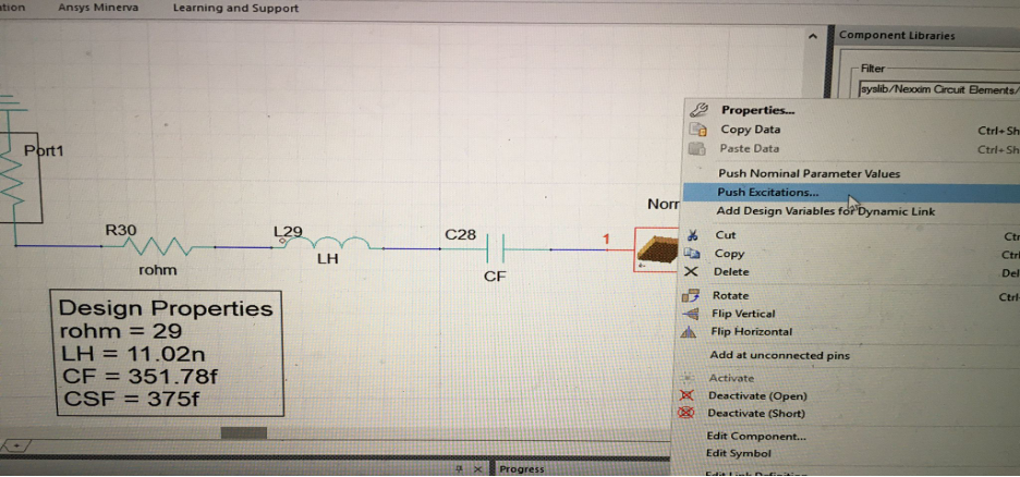
My question is how to properly prepare this for fabrication through layout in HFSS circuits. I am still new to HFSS circuits so yeah, when I click on layout editor it shows me this:
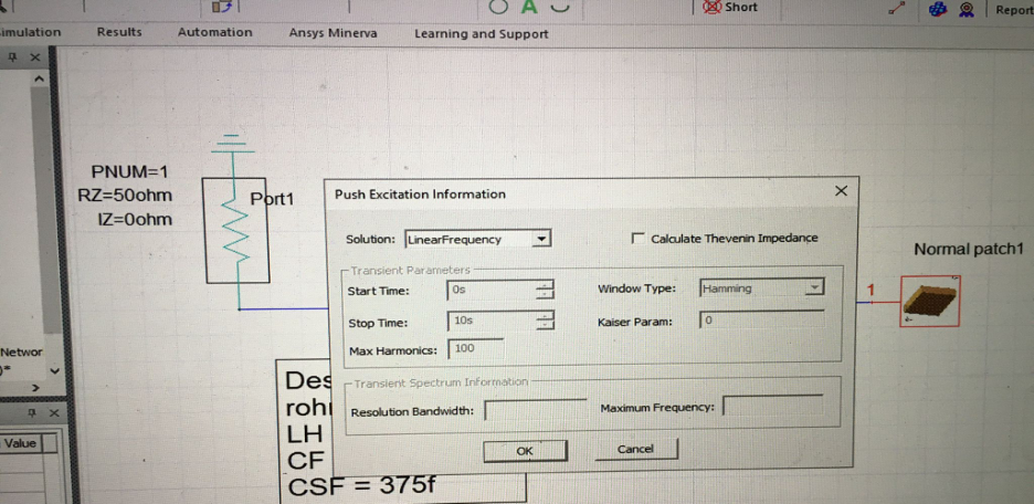
so i am just trying to make sense of all of this, I have worked on layouts in ADS in the past but not extensively in HFSS. when I right-click on my imported antenna design it shows me an option to "push excitation" i assume to the original design like this:
But my question is what will that do exactly? for the project i plan to end up using an SMP connector and its receptacle like this for feeding the antenna:
https://www.digikey.ca/en/products/detail/pulse-electronics/W9011M/8555426?utm_adgroup=&utm_source=google&utm_medium=cpc&utm_campaign=PMax%20Shopping_Product_New%20Customer%20Acquisition&utm_term=&productid=8555426&utm_content=&utm_id=go_cmp-19909744982_adg-_ad-__dev-c_ext-_prd-8555426_sig-EAIaIQobChMIp--qydKrhAMVe01HAR0T-wJWEAQYCCABEgLXk_D_BwE&gad_source=1&gclid=EAIaIQobChMIp--qydKrhAMVe01HAR0T-wJWEAQYCCABEgLXk_D_BwE
https://www.digikey.ca/en/products/detail/te-connectivity-amp-connectors/2337019-1/9974052
Â
Thank you as you get back to me.
-
February 20, 2024 at 5:03 pm
Praneeth
Ansys EmployeeHi Samad,
Thank you for reaching out to the Ansys learning forum. Your patience is much appreciated.
Please go through this AIS free video tutorial on doing cosimulation between HFSS and Circuit inside the AEDT - Cosimulation Using Ansys HFSS and Circuit - Lesson 2 - ANSYS Innovation Courses.Â
Best regard,
Praneeth Munaga.Â
-
February 20, 2024 at 5:26 pm
Samad Atta
SubscriberHello Praneeth,
Â
I want to first say thank you for your reply but i have already seen this video and i know everything i need to know about this video already. This doesn't answer my questions, unfortunately, leaving me in the same place. Can i get access to more specialized help? please?
-
-
February 21, 2024 at 6:26 am
Praneeth
Ansys EmployeeHi Samad,
It is great to know that you have already watched the suggested video. From the post, it was not clear whether you had questions on designing a matching network or how to do cosimulation. So, that video was suggested.Â
Please share your exact questions and we will try to clear them to the extent possible.
Best regards,
Praneeth. -
February 21, 2024 at 6:43 am
Samad Atta
SubscriberHi Praneeth,
In short, I am trying to make my layout make sense for fabrication, I have a matching network as shown in the pictures of my original post.Â
-
February 21, 2024 at 7:05 am
Praneeth
Ansys EmployeeÂ
Hi Samad,
For fabrication, you need to export the layout of your CAD model from Ansys HFSS. Please check with your fabrication team on which file formats are supported.
You have designed a matching network in Ansys Circuit which means that this matching network will be connected externally to the antenna and can be connected after fabrication. This tool gives the combination required for the matching network but will not generate the layout for connection.
If you intend to design the matching network on the same pcb of antenna then they should be added in the Ansys HFSS design itself.
Best regards,
Praneeth.Â
-
February 21, 2024 at 7:16 am
Samad Atta
SubscriberPraneeth,
Okay, so how do I add the matching network to the ANSYS HFSS design itself? by pushing excitation? thank you.
-
-
February 21, 2024 at 3:58 pm
Praneeth
Ansys EmployeeHi Samad,
"Push excitation" modifies the excitations in HFSS as per the response of the matching network.
For designing the lumped elements required for matching netwrok, you can use "lumped RLC Boundary" in Ansys HFSS. Please go through the published papers and literature on designing the matching network.
Best regards,
Praneeth.Â
-
February 21, 2024 at 4:03 pm
Samad Atta
SubscriberPraneeth lumped RLC does not do series but only parallel so it's not the same. I explored the "lumped RLC Boundary" route before I embarked on my HFSS circuits journey.
-
-
February 21, 2024 at 6:12 pm
Praneeth
Ansys EmployeeYou can assign separate RLC boundaries for each of the elements and assign only a single element per boundary for each of the elements in your matching network and connect them. In the physical model, you will have these as individual elements rather than a combination.
However, It is also possible to select series connection in the lumped RLC boundary window.
Hope this helps.
Best regards,
Praneeth.-
February 21, 2024 at 7:51 pm
Samad Atta
SubscriberHello,
Yes i was thinking about the first suggestion you have for me but that can be faulty, about selecting a series RLC instead of a parallel/lumped one can you guide me on how that is done? thanks
-
-
February 22, 2024 at 6:28 pm
Praneeth
Ansys EmployeeHi,
You can select the series or parallel connection in the Lumped RLC boundary window itself.
Best regards,
Praneeth.
-
- The topic ‘converting my HFSS circuit to layout or pushing excitation to 3D-modeler’ is closed to new replies.
- Lumped Port Deembed
- Hfss 3D pcb via capped and filled with epoxy
- HFSS libnvidia-ml.so too old or could not be found – Warning in slurm job output
- Optimizing Via Impedance in Ansys HFSS 3D Layout Using Geometric Parameter Sweep
- AEDT Natural Convection with default correlation is failing solver initializatio
- STL Import Errors in HFSS After Cleaning in SpaceClaim
- Three-Phase Voltage Imbalances in dual stator electric generator
- Calc Error in Field Calculator after PyAEDT Analyze
- import file autocad 3d
- Co-simulation in Q3D, Icepak – meshing problem
-
3942
-
1414
-
1272
-
1119
-
1015
© 2025 Copyright ANSYS, Inc. All rights reserved.