-
-
August 21, 2024 at 2:17 pm
ph23resch01002
SubscriberDear Sir/Madam,
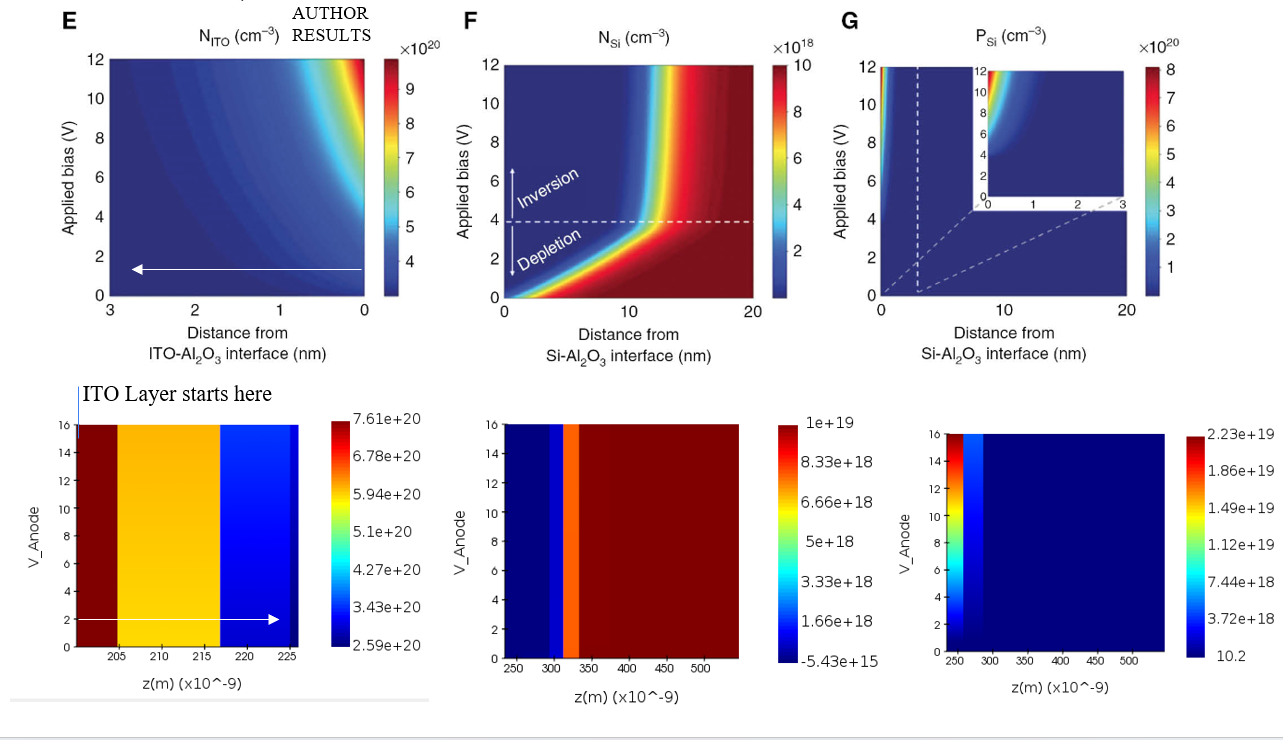
I am attempting to reproduce the results from the article "Tunable all-dielectric metasurface for phase modulation of the reflected and transmitted light via permittivity tuning of indium tin oxide." In the article, they used Lumerical Device to perform the simulations. I have attached the unit cell provided in the paper alongside the unit cell I designed using Charge simulations.
The unit cell consists of a SiO2 substrate, on which a Si slab is placed. On top of the Si slab, there is an ITO layer, followed by an Al2O3 layer, and finally, doped-Si resonators. Using the electrical connection boundary condition, the voltage is applied between the doped-Si resonator and the ITO layer. The electrical properties of the Indium Tin Oxide (ITO) and the doped-Si were mentioned in the supplementary notes of the article. I used those properties to create the ITO and doped-Si in the material section.
In the article, ITO was degenerately doped with an n-type dopant at a concentration of 3*10^20 cm^-3, and the doped-Si was doped with an n-type dopant at a concentration of 1*10^19 cm^-3. I used constant doping as it was mentioned that the ITO and doped-Si were uniformly doped in the supplementary notes. With constant doping, I ran the simulation and encountered a "Job right error." To resolve this, I changed the doping method from constant to diffusion doping and was able to run the simulations.
After doping the ITO and Si resonators, I attempted to sweep the voltage from 0 V to 16 V to observe the charge distributions. However, the results I obtained do not match the results in the article I am trying to reproduce; there is a significant discrepancy. I have attached both my results and those from the article for comparison.
Could someone please advise on what the potential error might be?
-
August 21, 2024 at 3:04 pm
Guilin Sun
Ansys EmployeeThank you for the detailed description. Accurately duplicating published results is very challenging, since not all the simulation information is available.
In your case, one obvious reason is the doping. The suspecious result is, it does not change with applied voltage (first two). You will need to check what causes this result except the 3rd one. I guess it is not from meshing. Where did you do the voltage sweep? if it is from the sweep object, you will need to check if the changing voltage is applied to the contact. If it is inside the contact, and it is normally there, you need to dig it out the reason: you only need to have two applied voltage values.
Make sure the material properties are correct.
-
- You must be logged in to reply to this topic.


-
3407
-
1057
-
1051
-
896
-
882

© 2025 Copyright ANSYS, Inc. All rights reserved.


