Ansys Assistant will be unavailable on the Learning Forum starting January 30. An upgraded version is coming soon. We apologize for any inconvenience and appreciate your patience. Stay tuned for updates.
Photonics

Photonics

Topics related to Lumerical and more.

Average E-field calculation on a fiber surface

    • atfkerem76
      Subscriber

      Hello. I'm simulating an optical antenna structure. There is a fiber in the center of the structure.

      I'm using a 3D monitor as it seems in the below image. 

      The source wavelength is between 360-345nm's and it's propogating along the "x" axis. After the simulation it shows me the E-field results on "z" axis as "slices". There are 53 datas in this index. And it changes depending on the position of slices. 

      I'd like to calculate average E-field on it's surface in "z" axis. Is there a way to do that? Thanks.

    • Guilin Sun
      Ansys Employee

      Definitely, you can. However, it seems you are simulating a fiber cavity? where the source is located? inside the cavity or outside? dipole or mode source or Gaussian source.

      Once you get the E-field from the 3D monitor, you can integrate along Z only. related scripts are

      getresult  eg E3D=getresult("monitor","E")

      dot operation  Ez3D=E3D.Ez  #Ez

                             E2=E3D.E2; # intensity

                            z=E3D.z

      integrate  eg integrate(E2,3,z);

      Please search online if you want to get more informtation for each script.

    • atfkerem76
      Subscriber

      Actually, not the cavity. There is an actual fiber there but it's hard to see a bit I think ? source is outside of the structure, it's located at x:-600nm , y: 0nm, z: 600nm. It's a plane wave source. Fiber is at the origin of simulation which is x:0, y:0 and z:0.  Whole simulation area geometry is xspan: 2000nm, yspan: 2000nm and zspan: 2000nm.

      I used the script you mentioned and attached the integration result to "last_result" variable. Then I visualized it. Here is what I get:

      I'm using 21 steps for the frequency band. When tried to see actual 3D monitor results, it gave me 53 datas for each frequency step. Now I can monitorize just frequency responses for "z" axis. I think this makes sense. 


    • Guilin Sun
      Ansys Employee

      Where the device has two more material interfaces alog the propagation axis, it can be called "cavity". I am glad to can visualize the result using script.

    • atfkerem76
      Subscriber

      Oh I see... Sorry I'm still learning. 

      I have a few more questions though.

      First, with the same script, I tried to visualize the average E-field values for "x" axis and I get the image below. It actually seems that it shows the fiber cavity, but I didn't understand why it shows like there two fibers? 


      Second, after the simulations I was able to see the E-field results like "1.23,1.03" etc. Like the first image I've sent. But after the integration process, when I tried to visualize results, it was like "1.14e-06, 9.92e-07". Like previous image I've sent. Why is it shows like this? And since the source's amplitude was "1", can I say there are some amplifications happens in some places on fiber? 

    • Guilin Sun
      Ansys Employee

      Please use dataset to create the image data so you will know which axis represents what quantity: https://optics.ansys.com/hc/en-us/articles/360034409554-Introduction-to-Lumerical-datasets

      There is no Amplification for linear simulation, as you can measure the transmission and reflection are smaller than 1. However, the electric field can be enhanced, due to interference, diffraction and reflection (forming cavity standing wave).

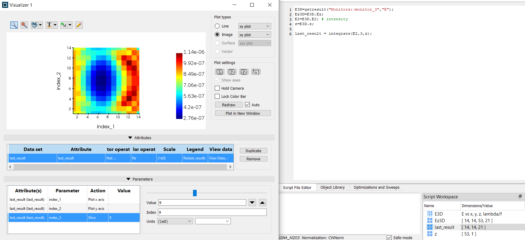
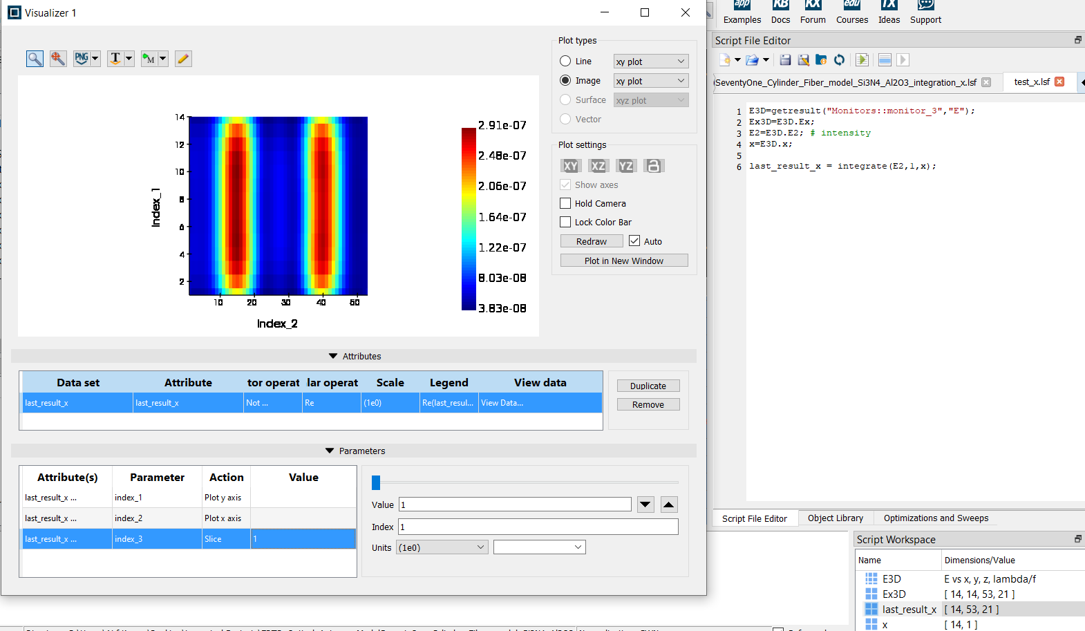
      Please note, you can normalize the intensity by dividing your current result with integrate(E2/E2,3,z). This way you can get relative field strength to the source amplitude. As you know the integration creates an additional length dimension.

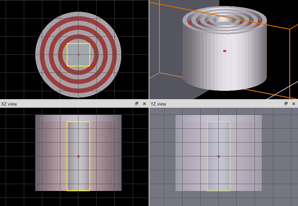
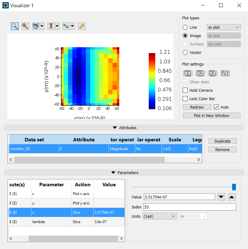
      Since this is cylindrical device, it has symmetry so you see two "bars". SO I guess the index_2 is along its diameter, index_1 is along its length? from your first image, the strong E-fields are not at the center.

      It is not supprising to me, as you are simulating a cavity, with a plane wave excitation. Do you use TFSF local plane wave, or regular plane wave with periodic boundary condition so you are simulating periodic array? if your device is a single section for fiber, please use TFSF: https://optics.ansys.com/hc/en-us/articles/360034902133-Understanding-source-normalization-in-the-TFSF-source

      If you use regular plane wave with PML, the PML will truncate the plane wave and then diffraciton occurs:

      https://optics.ansys.com/hc/en-us/articles/360034382874-Understanding-field-truncation-issues-with-finite-sized-plane-wave-sources

      I guess in  experiment you mayuse a gaussian beam, which has finite size, even though its beam waist is larger than the finer cross section. I think TFSF is a better choice for such case.


    • atfkerem76
      Subscriber

      I see. Many thanks for all these information. Learned a lot from this. 

Viewing 6 reply threads
  • The topic ‘Average E-field calculation on a fiber surface’ is closed to new replies.
[bingo_chatbox]