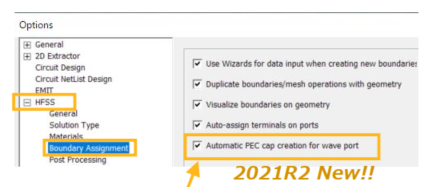
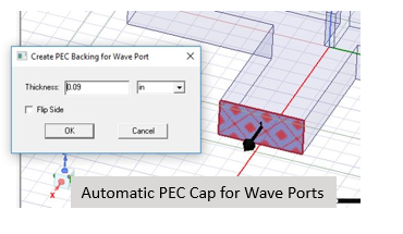
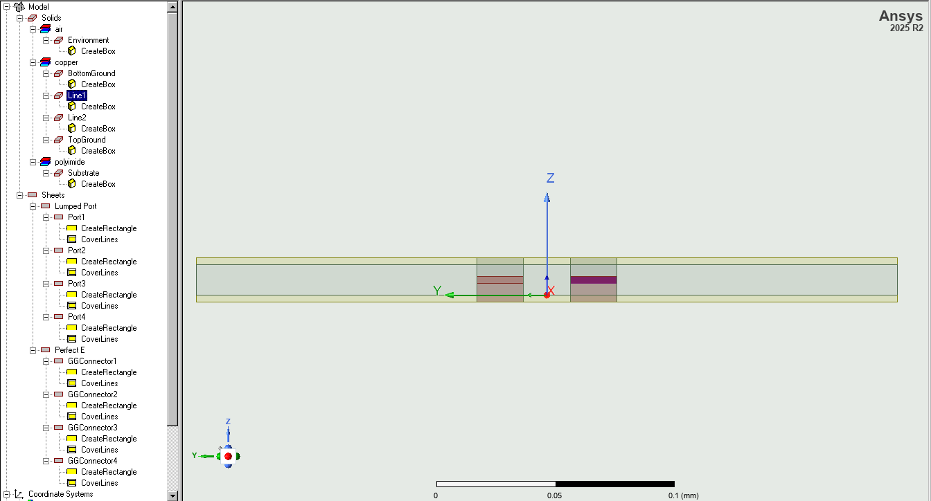
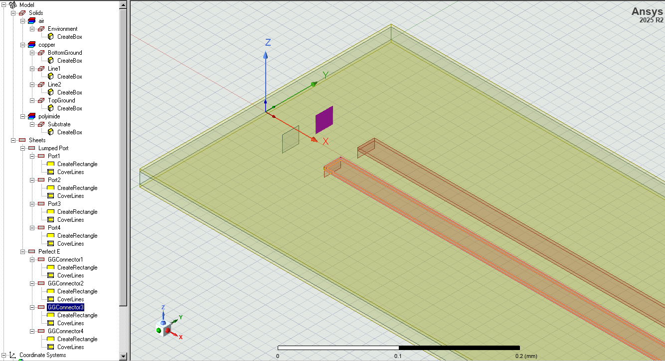
Ansys Assistant will be unavailable on the Learning Forum starting January 30. An upgraded version is coming soon. We apologize for any inconvenience and appreciate your patience. Stay tuned for updates.
Electronics

Electronics

Topics related to HFSS, Maxwell, SIwave, Icepak, Electronics Enterprise and more.

Edge couple microstrip

    • vagadiya
      Subscriber

      I am working on edge couple microstrip, which is inside solution space. For that I can not use wave port and I have to use lumped port. I am using 4 terminal lumped ports and then I define 2 differential lines D1 and D2. Now my question is how can I short-circuit my top ground plane and bottom ground plane? Without short-circuit this ground planes it doesn't make any sence. Thank you.

    • Takeshi Itadani
      Ansys Employee

      If you want to place a Wave Port inside the analysis space, you can perform the analysis by touching one side of the Wave Port to a pec object.
      If you are using version 2021R2 or later, a setting has been added to automatically create a pec object.


    • vagadiya
      Subscriber

      Thank you for your reply. Is there any way that I can do this with lumped port?

    • Takeshi Itadani
      Ansys Employee

      Lumped Ports are originally placed within the analysis space, so there is no problem with the usual placement method.
      If there are GND layers above and below, like in a stripline, use the one closer to the transmission line (the one with stronger electromagnetic field coupling) as the reference.
      If you feel that the upper and lower GND layers are the transmission line, then there should be no problem using the GND on either side as the reference. If you are really concerned, you can connect the upper and lower GND layers using a sheet with Perfect E boundary conditions set near the sheet where you set the Lumped Port, and use that connected sheet as the reference for the Lumped Port.

    • vagadiya
      Subscriber

      Thank you so much. This would be really helpful.

    • vagadiya
      Subscriber

      After implementing your suggestion I have my design as shown in attached photos. Here in 1st photo lumped port is in reference with BottomGround and 2nd photo GGconectors are plain sheet(assigned as PerfE boundary condition) which connects both ground plane top and bottom. Is this the correct way to do this?  

    • Takeshi Itadani
      Ansys Employee

      In the second image, is the purple highlighted sheet the one where you set the Perfect E boundary condition? If so, I think you should set the Lumped Port using that sheet as the Reference.
      There doesn't seem to be any particular problem with the first image.

    • vagadiya
      Subscriber

      Yes, I set perfect E boundary condition in 2nd image. But to set lumped port using that sheet as the reference is quite chaotic design, because port planes should be perpedicular to microstrip. So for that I have to set lumped port as I did and connect one more plane to connect this port plane and Ground-connector plane. I did that already and in that situation I got 99% reflections on port. So how can I deal with that?

    • Takeshi Itadani
      Ansys Employee

      Using the cross section of the first image, why not place the Perfect E boundary condition sheet connecting the upper and lower GND layers next to the transmission line, and then set up a Lumped Port between the transmission line and the sheet? This would then be perpendicular to the stripline.

    • vagadiya
      Subscriber

      Thank you. This is practical now.

Viewing 9 reply threads
  • You must be logged in to reply to this topic.
[bingo_chatbox]