TAGGED: lumerical, Lumerical-EME
-
-
May 27, 2025 at 10:31 am
512105003
SubscriberHi,
I have designed a 1x2 splitter using the EME solver and attached a screenshot. I'm having trouble determining the appropriate dimensions for the ports. Could you provide guidance on what I should consider when choosing these dimensions? Additionally, I'm unsure about using the "use full simulation span" option. When this option is checked, it seems the ports automatically extend to match the EME simulation region, as shown in the screenshot. However, when I manually set different x-span and z-span values for the port, the resulting S-parameter values change. Is this expected behavior? Also, when using the "use full simulation span" option, the S-parameters (Abs^2 values) for S21 and S31 both yield 0.9834. I'm not entirely sure how accurate or reliable these results are. Could you provide any insight into this? I would greatly appreciate any clarification or best practices on setting port spans to ensure accurate simulation results.
-
May 27, 2025 at 9:29 pm
Amrita Pati
Ansys EmployeeHi,
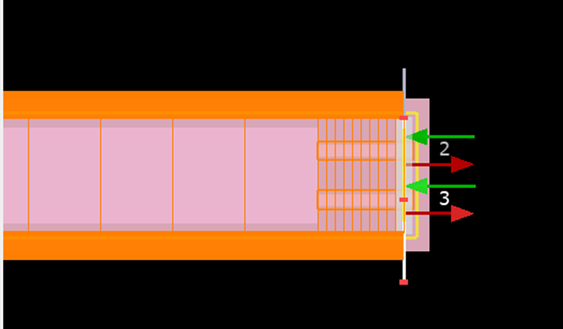
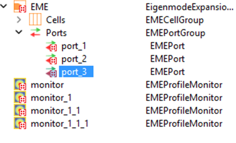
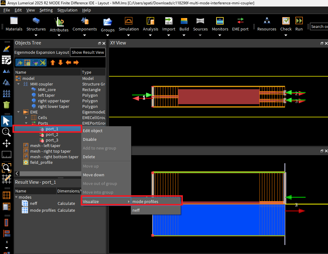
Since you have multiple waveguides at the output, I will recommend using two separate ports that do not span the length of the entire simulation. When you have both the ports spanning the entire length (I believe y-direction in this case), you are most likely selecting the same mode for both the ports. The modes are calculated based on the entire source cross-section of the ports and the cross-sections will be the same for Port 2 and Port 3. If you’ve selected the “fundamental mode” as the “mode selection” field (which is the default) for each port, then the same mode will be calculated for both the ports as the cross-section (and the geometry within that cross-section) is same. You can confirm that by visualizing the mode at Port 2 and Port 3.
If they are the same mode, then it’s plausible that S21 and S31 are same.
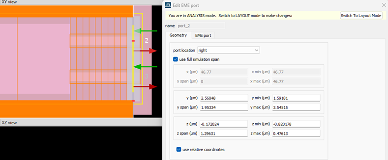
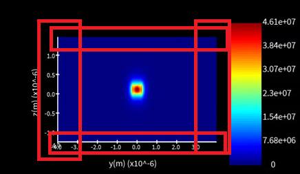
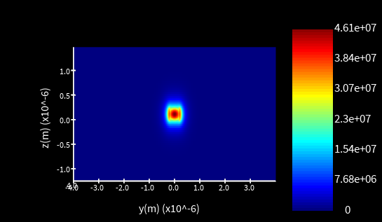
As I mentioned, my recommendation will be to have two ports, separately over each output waveguide (not the entire simulation length) as shown here. Visualize (as shown in the screenshot above) the mode profiles from each port before you run the simulation to make sure that the correct modes are being used. Now coming to the size of the ports. Visualize the mode at each port and ensure that the fields have fallen to ~1e-04 (or smaller) of the peak. This is to make sure there is limited to no diffraction at the edges of the source. As shown in the screenshot below, the fields are ~ 0 at the edges of the source:
The results won’t change if you increase the source span beyond that but I will recommend making sure that the other waveguide is not included within the source span of the first and vice-versa. Please feel free to let me know if there are any questions.
Regards,
Amrita -
May 29, 2025 at 1:18 pm
512105003
SubscriberHi,In your response, you mentioned that I should “visualize the mode on each port and make sure that the peak of the fields falls to ~1e-04 (or smaller)”. I would like to clarify what this means in practice.For instance, in the example image you shared, the peak value appears to be around 4.61e+7. Could you please explain what exactly is meant by "peak value" in this context? Additionally, how should I verify that the field amplitude has decayed to approximately 1e-04 (or smaller) relative to this peak? Thank you in advance. -
May 29, 2025 at 10:50 pm
-
- You must be logged in to reply to this topic.
-
3246
-
1031
-
969
-
859
-
798
© 2025 Copyright ANSYS, Inc. All rights reserved.