TAGGED: helical-antenna, hfss
-
-
November 10, 2024 at 3:59 pm
kagankarakusx
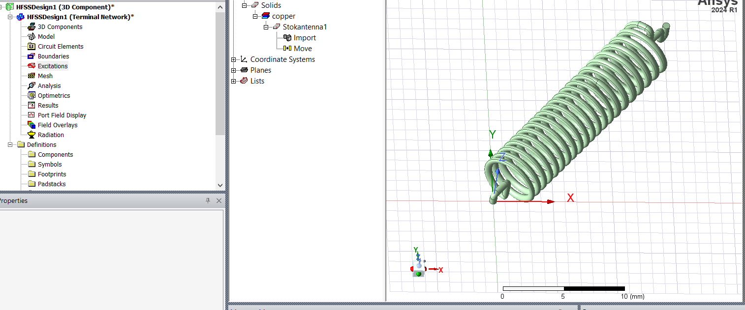
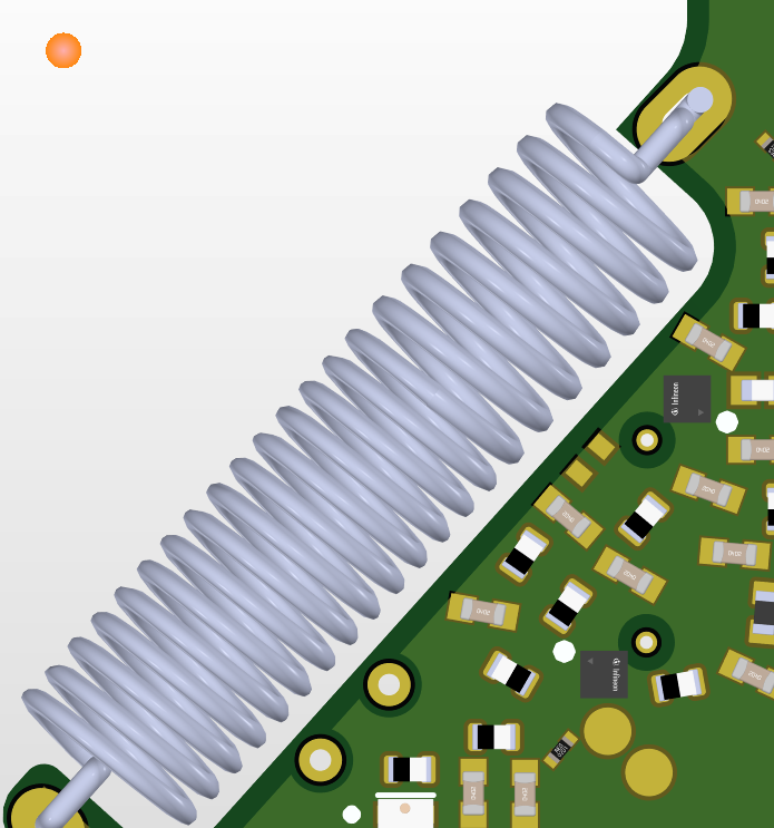
SubscriberHello, I have previously simulated chip antennas and nfc antennas using hfss and I adjusted the rlc lumped ports and made the antennas resonate with tuning in the circuit section.This time I want to simulate with a helical antenna design.I have the 3D step file of the antenna.Here is what I want to do.Finding the s11 characteristics of the antenna.(only by assigning a small reference plane on its own maybe)Finding the s11 characteristics by taking the antenna pcb gnd as reference.Extracting the s11 parameters by analyzing the antenna from the tuning circuit input on the pcb.For this, after importing the pcb from siwave, I can import the helical antenna as a step file.and then I can assign the copper feature.Or I can save the helical antenna as (.a3dcomp) and bring it to the hfss where the pcb is located as a component.I am not sure which one is correctThe point I can't understand is how can I connect the feed tract antenna output point of the pcb. Because the helical antenna will be soldered to the pcb. Please help.Especially when extracting the S11 parameters from the IC feed point, I need to define in the program that the copper helical antenna touches the PCB from the through hole point.

-
November 11, 2024 at 3:40 am
Kihyun Kong
Ansys EmployeeHi Kagankarakusx,
It makes no sense to extract the S11 of an antenna based on a small reference during the workflow you have in mind.
Electrical small antennas are highly affected by the ground.
These antennas have the same behavior as a monopole, so you need to think in terms of Image Theory.
Therefore, you need to create an simulation model that combines the actual PCB and the antenna.
Using a 3D component has the advantage of being reusable, and there is no difference between using a step file directly from the current analysis model or using a 3D component.
To join the helical coil to the PCB, you can create a box to connect the PCB and coil to unite them, taking into account that soldering is used in the real model. The size of the solder doesn't have a big impact, so you can create a box of the appropriate size.
-
- You must be logged in to reply to this topic.


-
5674
-
1890
-
1419
-
1305
-
1021

© 2026 Copyright ANSYS, Inc. All rights reserved.


