-
-
August 31, 2021 at 3:16 pm
Raikage97
SubscriberThe results reported in this example:
are inchoerent with the result of the simulation. I didn't modify any parameter, I just ran the code.
September 2, 2021 at 2:25 amGWANG
Ansys EmployeeSeptember 4, 2021 at 4:05 pmRaikage97
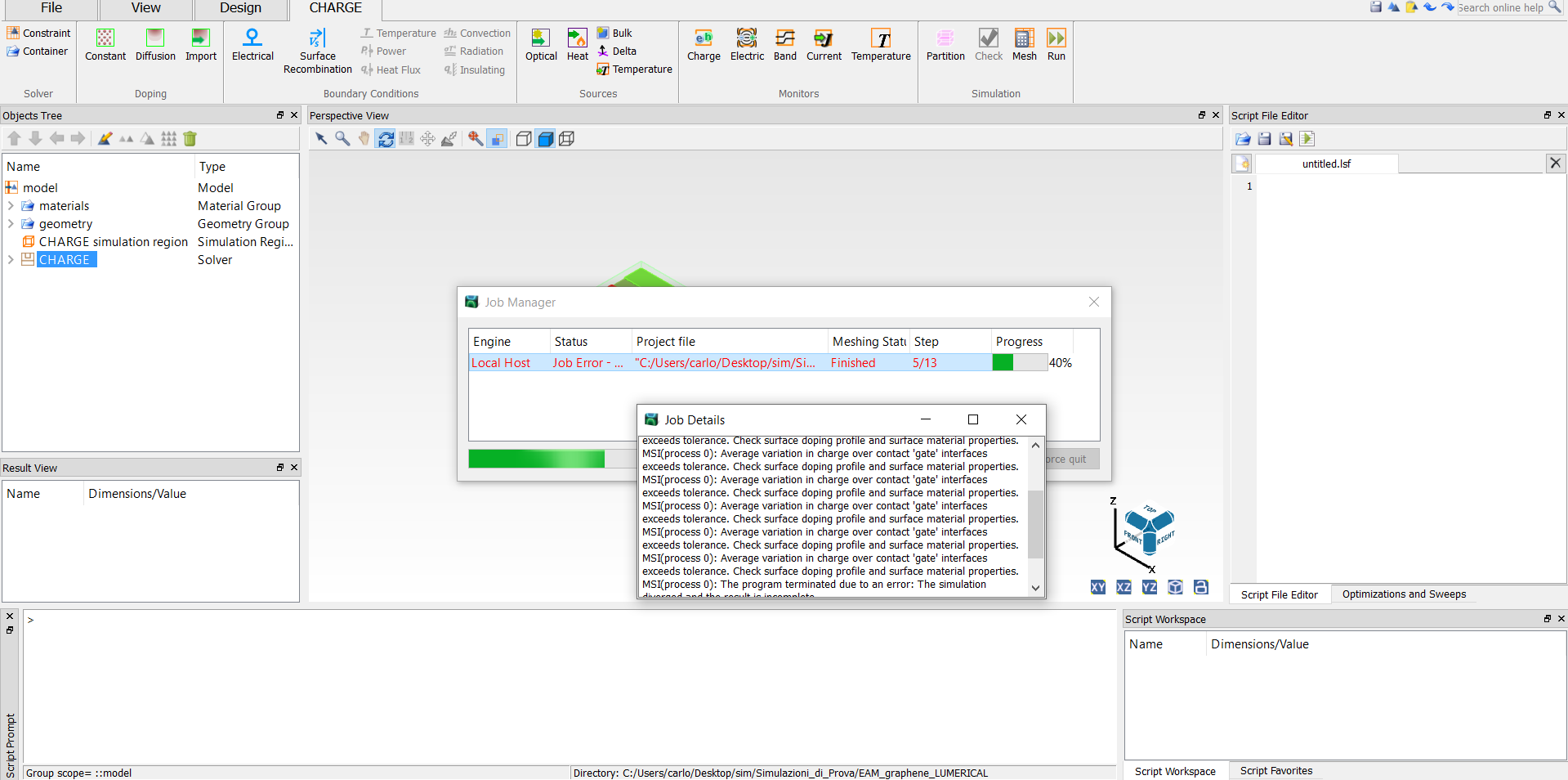
SubscriberYes sir. When I run the code graphene_electro-optic_modulator_1, I have the following error:
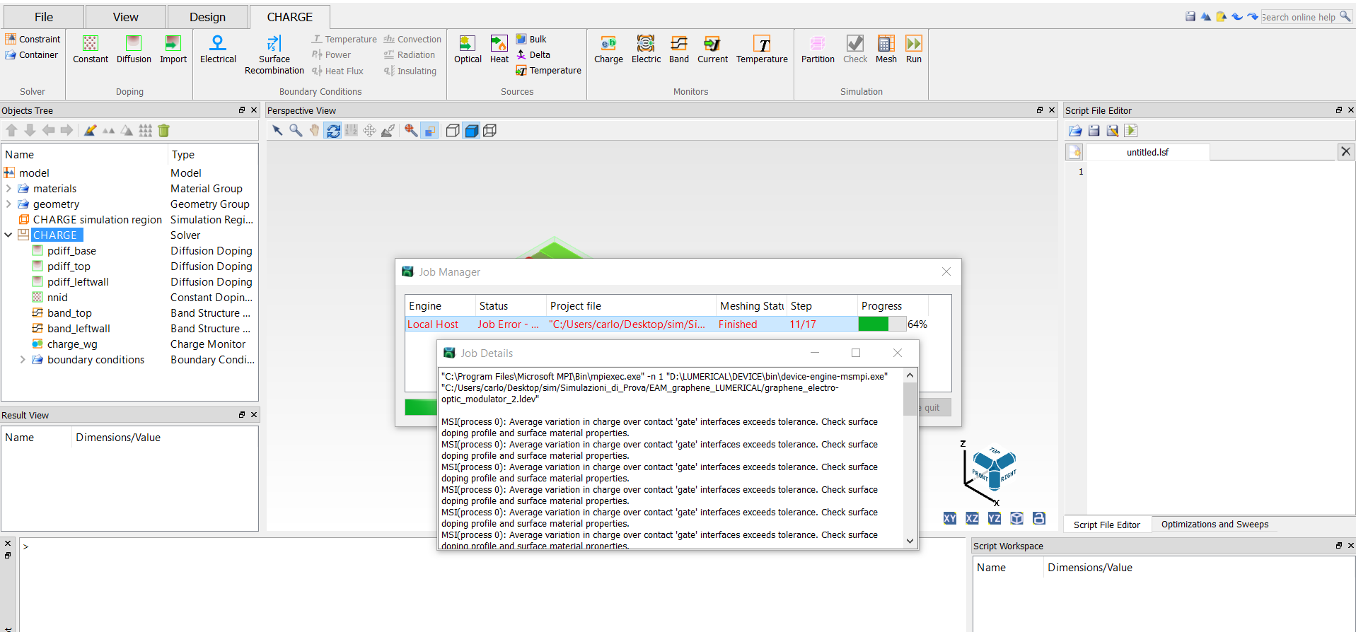
 When I run graphene_electro-optic_modulator_2, I have the following error:
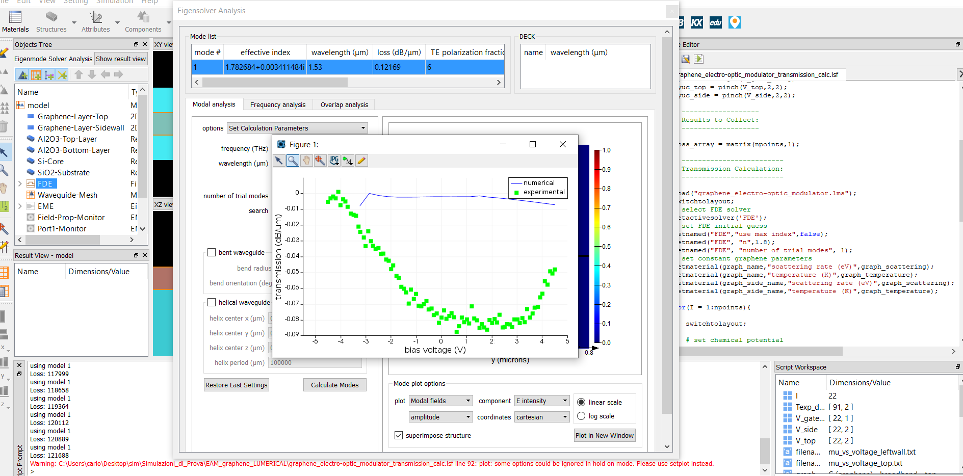
 The same of the first one. After getting the simulation data using script get_top_Ef_data.lsf and get_leftwall_Ef_data.lsf, running code graphene_electro-optic_modulator_transmission_calc.lsf I get the following result:

Simply put, I can't get your results.
I am also curious to know in detail, if it is possible, how the parameters m* and Ec were derived to schematize graphene on DEVICE.
Moreover in the article it is stated that the guide is single mode, but actually performing the simulation with FDE more modes appear. How is this possible?
September 9, 2021 at 7:42 pmkghaffari
Ansys EmployeeHi Carlo,
Thanks for posting this. I tested the example and can confirm thereÔÇÖs a geometry creating issue in the version 2021 R2.1 when running the CHARGE project files. We recommend downgrading to previous major release 2021 R1.x. I tested the example in 2021 R1 and it works in that version. Sorry for the inconvenience.
For m* and Ec, their derivation is described in detail in the example. Basically, they are used as fitting parameters to match the density of states between the 2D and 3D model.
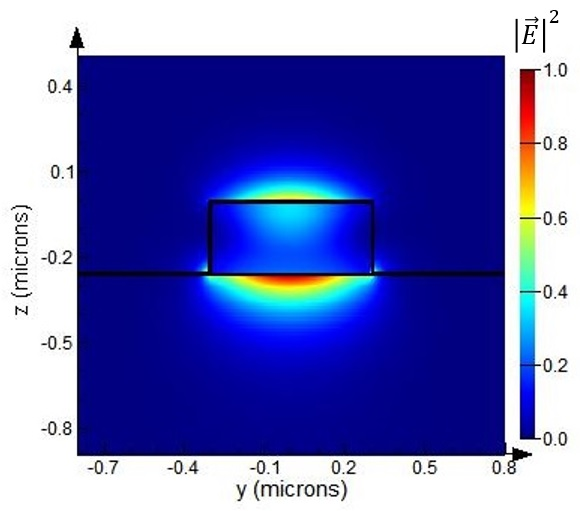
Regarding the mode, we indicate the mode that the device has been intended to operate for:
 This is the mode the consequent calculations and derivation of transmission is based on.
All the best Khashayar
September 9, 2021 at 8:36 pmRaikage97
SubscriberSeptember 9, 2021 at 8:39 pmRaikage97
SubscriberThanks kghaffari, I will try to do what you told me.
Best regards Carlo
September 14, 2021 at 7:16 pmRaikage97
SubscriberI tried to do what you said, but I still have the same error:
"average variation in charge over contact 'gate' interfaces exceeds tolerance. check surface doping profile and surface material properties "
By changing the thickness of the graphene and varying the fit parameters, I still have the same error, but the simulation tends to go little further
September 21, 2021 at 7:34 pmkghaffari
Ansys EmployeeFor future reference: we confirmed the example can be run fully with the mentioned version of the software.
Viewing 7 reply threads- The topic ‘Example error- EAM graphene based’ is closed to new replies.
Ansys Innovation SpaceTrending discussionsTop Contributors-
3762
-
1333
-
1168
-
1090
-
1014
Top Rated Tags© 2025 Copyright ANSYS, Inc. All rights reserved.
Ansys does not support the usage of unauthorized Ansys software. Please visit www.ansys.com to obtain an official distribution.
-


Ansys Assistant

Welcome to Ansys Assistant!
An AI-based virtual assistant for active Ansys Academic Customers. Please login using your university issued email address.
Hey there, you are quite inquisitive! You have hit your hourly question limit. Please retry after '10' minutes. For questions, please reach out to ansyslearn@ansys.com.
RETRY


