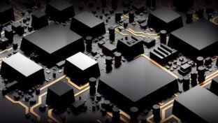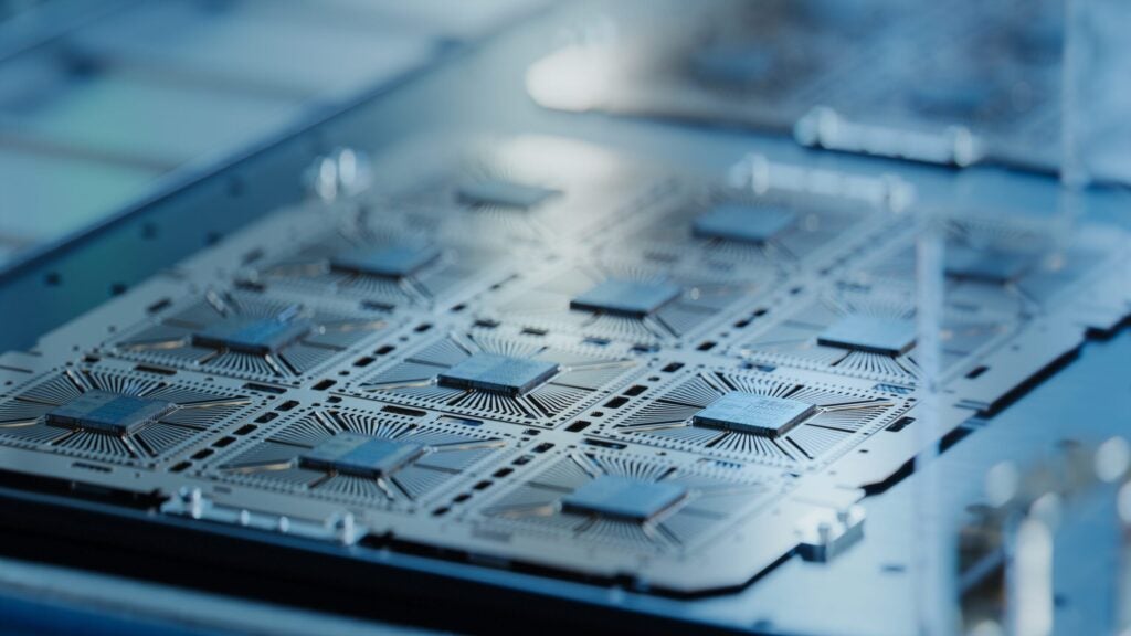
Welcome to the Multi-Die Semiconductor Integrity Course! This comprehensive 10-lesson course is designed for engineers, designers, and technology enthusiasts seeking to master the intricacies of multi-die systems—a rapidly emerging area at the forefront of semiconductor innovation. As advanced technologies like 2.5D and 3D integration revolutionize the industry, understanding the challenges and opportunities of multi-die architectures has never been more critical.
In this course, you will learn:
- Foundations: Explore the evolution of multi-die systems and their key components like TSVs, RDLs, and interposers.
- Advanced Packaging: Discover how technologies like TSMC CoWoS, Samsung I-Cube, and Intel Foveros drive high-performance integration.
- Performance Challenges: Address power, thermal, signal, and structural integrity in multi-die designs.
- Innovations: Dive into Co-Packaged Optics (CPO) and High-Bandwidth Memory (HBM) shaping AI, HPC, and 5G.
- Design Standardization: Learn about 3Dblox and 3DCODE, the languages simplifying multi-die design workflows.
- Simulation Tools: Leverage Synopsys solutions for Multiphysics analysis to ensure robust and reliable designs.
From foundational principles to real-world applications, this course provides everything you need to design, analyze, and optimize multi-die systems. Whether you’re an engineer, designer, or enthusiast, this course will transform your understanding of modern semiconductor design.
Join us and take the leap into the future of multi-die technologies!
-
Cost: FREE
- Course Duration: 4-6 HOURS
- Skill Level: Beginner
- Skills Gained: Understanding of advanced semiconductor packaging technologies, including 2.5D and 3D integration, with emphasis on multi-die architectures, their challenges, and opportunities in modern electronic design.
No reviews available for this learning resource.