Electronics

Electronics

Topics relate to HFSS, Maxwell, SIwave, Icepak, Electronics Enterprise and more

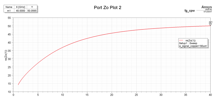
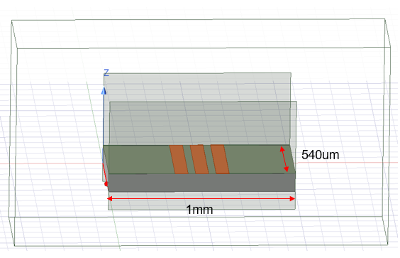
Zo when applying bulk conductivity to the silicon substrate of finite-ground CPW

    • 경민 ì‹ 
      Subscriber

      A SiO2 dielectric layer is placed on a silicon substrate, and on top of that are ground and signal planes made of copper.

      The silicon substrate is 100 μm thick, the SiO2 layer is 700 nm thick, and the ground and signal planes are 1 μm thick.

       The structure is ungrounded, meaning there is no ground plane beneath the substrate.

      When a conductivity of 10 S/m is applied to the silicon substrate made of Si material, the characteristic impedance appears symmetrical about the X-axis. 

      Is this normal if I want to adjust it to achieve 50 ohms?

    • DMARATHE
      Ansys Employee

      Hi,

      Thanks for posting your query on forum.

      I am not very sure with limited information why the characteristic impedance graph is coming like that.

      However, I have few suggestions. It is seen that S-parameters and port impedaces changes with wave port size. The right size of wave port and placement is recommened to avoid getting excited parallel plane waveguide mode.

      Some recommenedtions :

      Port width should be no less than 3 x the overall CPW width, or 3 x (2 g + w)  

      Port height should be no less than 4 x the dielectric height, or 4 h

      The wave port outline must contact the side grounds and should not exceeing lambad/2 in any direction

      g = spacing between signal and ground trace, w = width of signal trace and h = substrate height

      Thanks,

Viewing 1 reply thread
  • You must be logged in to reply to this topic.