-
-
December 18, 2023 at 10:45 am
handon
SubscriberHello,
I want to ask about planar silicon solar cells with metal grid electrodes.
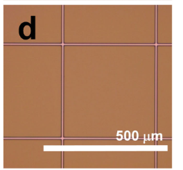
My objective in this simulation is the calculation of shading loss resulting from the metal electrode area.The simplest way to fabricate this structure is just fabricating the whole 3D unit cell.
However, it required many resources in FDTD and CHARGE when the spacing of the mesh grid is 50 um or more. So I set up the simulation processes like below:
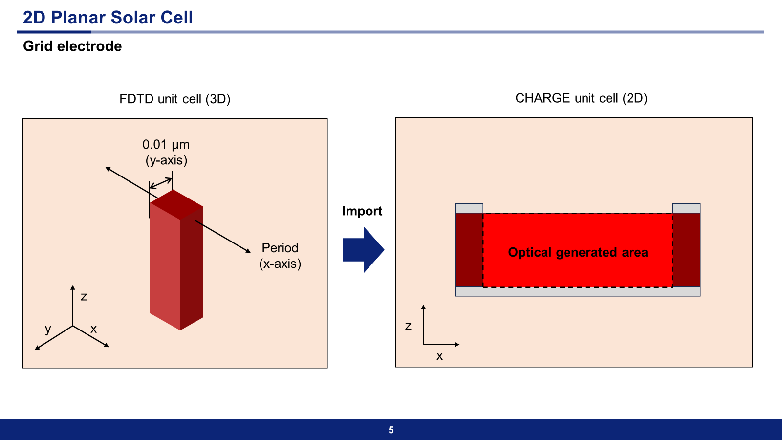
1) FDTD
I set the small FDTD region and enabled the 'period' in the optical generation rate (ogr) analysis group in FDTD.The result of the simulation calculates ogr of the Si substrate enlarged to the x-axis.
2) CHARGE
Parallel metal lines are located at the left and right ends in the x-axis. (For enlargement in the y-axis, I couldn't set the metal grid.)
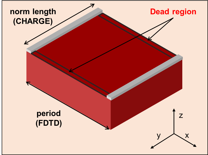
Then, the solar cell is expanded again in the y-axis as 'norm length' in 'CHARGE'.The above process makes it possible to simulate a 3D solar cell with metal electrodes, but it is not grid electrodes.
As you can see in the picture, the designed 3D solar cell has a dead region where it has no ogr data and no electrode.How can be possible to simulate a solar cell with mesh electrode even if the spacing of metal grid is large?
Theoretically, it can be possible but it requires a lot of resources. Can you let me know another way to simulate with fewer resources? -
January 5, 2024 at 10:47 pm
Amrita Pati
Ansys EmployeeHi Handon,
I sincerely apologize for the late reply. We seem to have missed your question.
Let me know if I understand the situation correctly. You have these grids in each unit cell. I assume that there will be a shadow under the metals where no light will be incident. In FDTD, you will have to do a 3D simulation. Then I think you can find an average of the generation rate over the cross-section so that it can be used in a 2D CHARGE simulation, similar to the approach used in the VPD example.
But I think you most likely will have to do a 3D CHARGE simulation as well. Do you expect the metal grid (also in the dead region) to have an impact on the electrostatic behavior of the solar cell? In other words, if you capture the generation rate from the 3D FDTD simulation, will you be applying bias to the entire grid?
The question with regard to reducing the resources, is it on FDTD or CHARGE or both?
Regards,
Amrita-
January 9, 2024 at 4:05 am
handon
SubscriberHi Amrita,
I'm glad to see you.
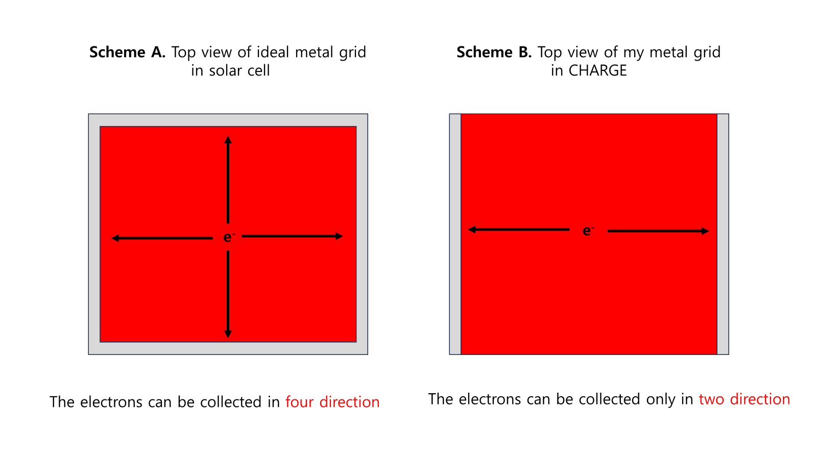
I hope the metal grid has an impact on the electrostatic behavior of the solar cell like scheme A.
To get the photovoltaic performance of solar cell, I will also apply bias to the entire grid.
However, it requires huge resources on FDTD and CHARGE when the spacing of the grid is approximately 50 um and above because the size of unit cell should be as large as the spacing of grid.
I set the unit cell design like scheme B because I don't know how to design a large mesh grid of solar cell with requiring fewer resources.
I hope you can fully understand my question.
If you want some more details, please reply about this.
-
-
January 10, 2024 at 10:09 pm
Amrita Pati
Ansys EmployeeHi Handon,
Good to see you too. Thanks for sharing more information, it's much clearer to me now. So you are correct we would need to do a 3D FDTD and 3D CHARGE simulation. There are a few things we can do to reduce the computational requirements. I will start with FDTD. I don't work on CHARGE a lot, so I will get my colleague's input on that side and come back with more information.
When it comes to FDTD, the most straightforward thing you can do of course is 1. reduce the mesh size. But that will definitely affect the accuracy of the simulation. In some cases, we might not require a high mesh density but it will be hard to predict that and will depend upon the specific use case. What I can suggest you to do is use a "Uniform Mesh" (as opposed to the default auto non-uniform), make the mesh coarser and compare the results to the default mesh of diffrent accuracies. If there is not a lot of difference in the results, you should be good to use the uniform mesh with a lower resolution. 2. I think you should use the symmetric and anti-symmetric BCs here. With this you can reduce the simulation domain by half or quarter depending upong whether you use them in one transverse direction or both. Please have a look: Symmetric and anti-symmetric BCs in FDTD and MODE. 3. You can also downsize the data collection of the monitors to reduce the hardware requirements. As shown below:
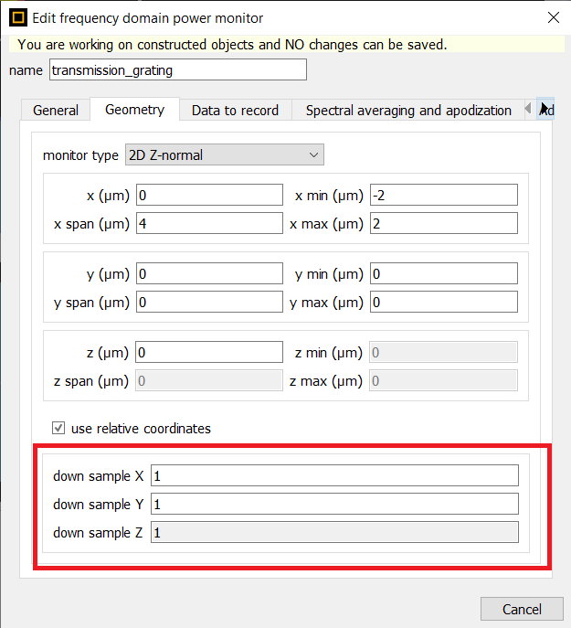
Increasing this number will reduce the number of points where the data is collected in each direction by that factor.
Regards,
Amrita -
January 11, 2024 at 5:31 am
Amrita Pati
Ansys EmployeeHi Handon,
I spoke to my colleague about CHARGE's hardware requirements. Unfortunately, in CHARGE there is not much we can do other that adjusting the mesh resolution. But same as FDTD we have to make sure that our results are within the reasonable limits of error with the use of coarser mesh.
Regards,
Amrita
-
- The topic ‘x-y metalgrid of solar cell in CHARGE’ is closed to new replies.


-
5814
-
1906
-
1420
-
1305
-
1021

© 2026 Copyright ANSYS, Inc. All rights reserved.

