-
-
May 21, 2025 at 8:40 pm
sanjum
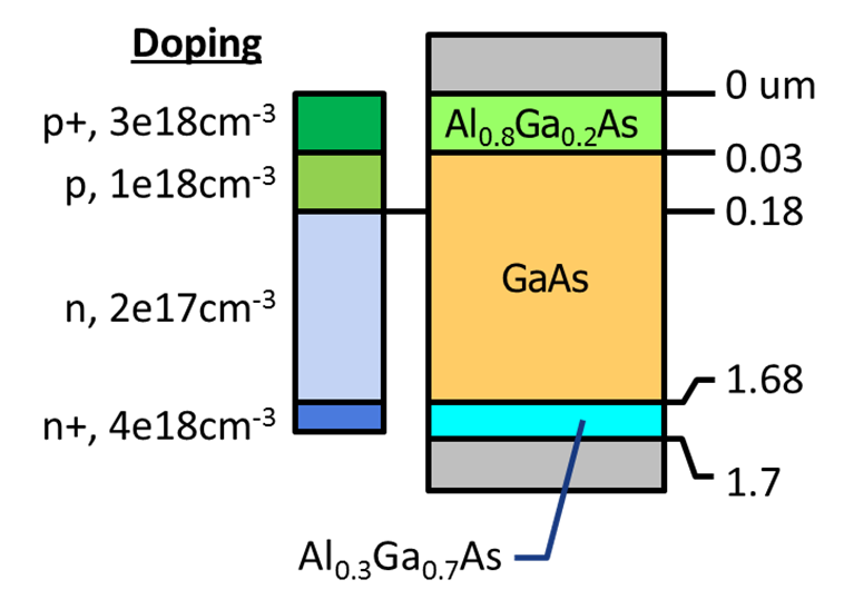
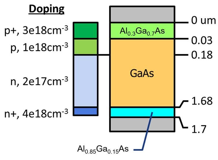
SubscriberI am examining the thin-film GaAs example, and it seems that in the simulation file, the geometry labeled nAlGaAs (with the material defined accordingly) overlaps with the p+ layer, while the pAlGaAs overlaps with the n+ layer. Is this an error?
When I switched the geometries and the materials accordingly, the efficiency dropped below the figures listed for the ideal case. I'm confused about what's going on. I was having trouble replicating the simulation results as provided in the article.
Could someone from Ansys clarify this? -
May 22, 2025 at 8:03 am
Niki Papachristou
Ansys EmployeeHi Sanjum,
Thank you for reaching out to us! Please note that this is the optics forum and not the photonics where lumerical related questions are posted. For your next lumerical question please post at: Ansys photonics forum. I will go ahead and transfer this post to the photonics forum.
Kind Regards,
Niki
-
May 23, 2025 at 3:06 pm
-
- You must be logged in to reply to this topic.


-
3492
-
1057
-
1051
-
965
-
942

© 2025 Copyright ANSYS, Inc. All rights reserved.


