-
-
April 28, 2022 at 5:14 pm
mgjeong
SubscriberI have designed GCPW (Coplanar waveguide with the ground) on a two-layered substrate.
The sweep frequency is between 500MHz to 2.5 or 3GHz.
The substrate used consists of a thin ferrite film (bias field is applied correctly) in 800nm to 3um scale on top of a 0.5 mm-thick dielectric.
To simplify the simulation, I used sheet PEC as conductors.
The goal was to reduce electrode width to somewhere comparable to the film thickness.
When I simulated same structure but with 1um-thick copper conductor layers instead of PEC sheets, the solution converged.
However, after reducing the electrode width to under 5um and applying sheet PEC conditions, my adaptive mesh does not converge.
If the thin ferrite film was solely causing the problem, I believe the previous simulations with wider conductors should have failed too.
But this only happens when the conductor and the thin film are both narrow and thin.
I need help from someone who knows meshing well.
** P.S. I have also tried inside-selection and on-selection mesh conditions too.
** Is there any way to force the mesh length in certain direction be fixed?
May 11, 2022 at 11:50 amPraneeth
Ansys Employee
Please provide more information to help us serve you better.
How many adaptive passes are set in the solution setup?
Can you increase the number of passes and check if it helps your case?
If possible share some screenshots of the model as it is not clear.
You cannot force the mesh length to only one direction but you can force it to all directions. This can still help your case.
You can also try solve for ports only (in the solution setup) to see it the simulation is setup correctly.
All the very best Praneeth.
May 11, 2022 at 6:31 pmmgjeong
Subscriber1.
am using 30 passes but it shoots error even before reaching to the number I set. Also, as it looks very unstable, I am setting "minimum converged passes" to 2 rather than 1.
2.
It did not help.
3.
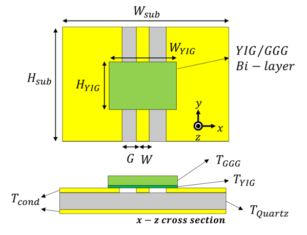
 I hope this schematic helps. I am designing a CPW line in a super thin substrate wafer (quartz). so T_Quartz is set around 10-20um. Accordingly, W and G must be set super small (sub-um) to meet our design goals.
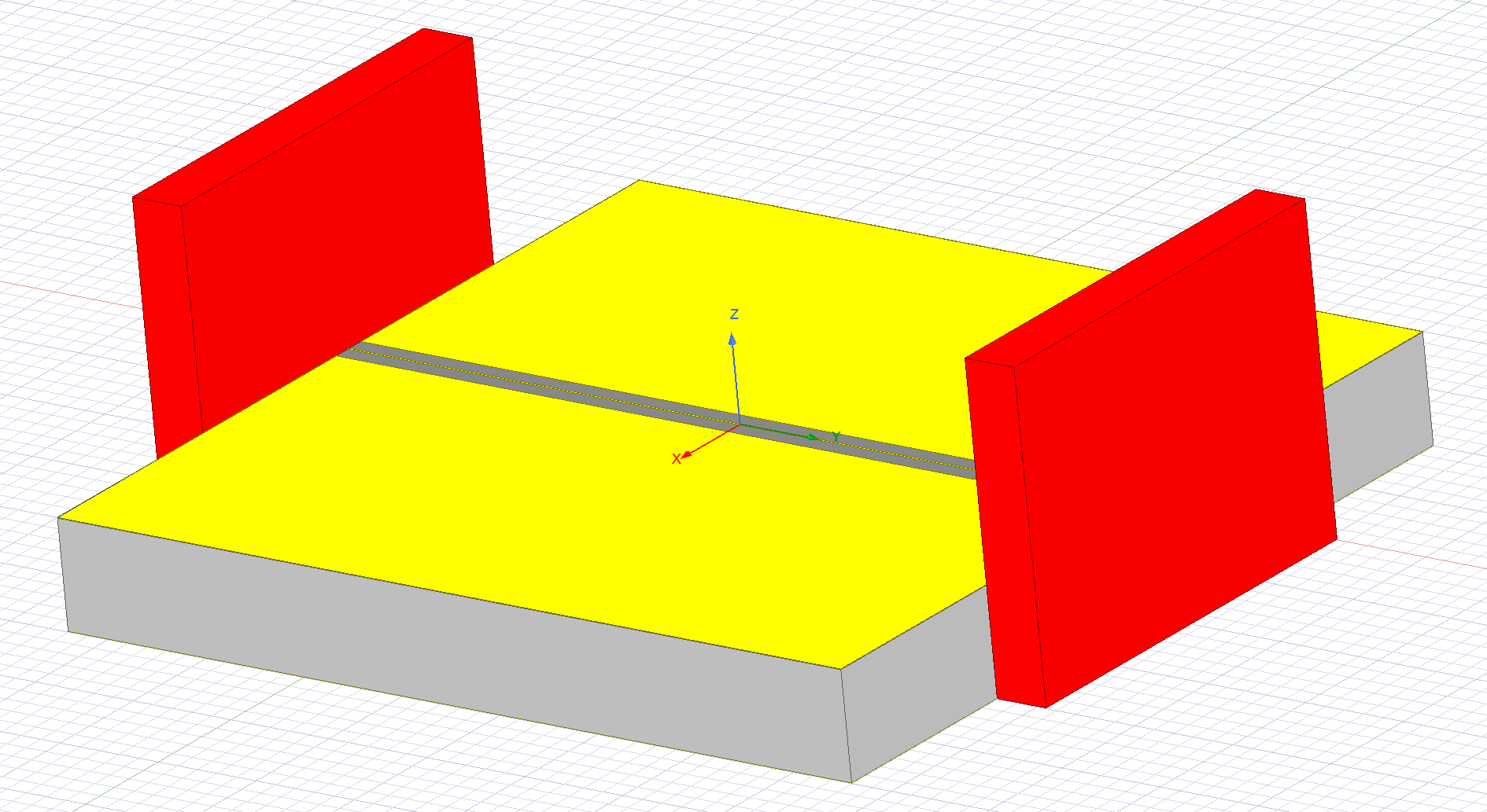
 This is a screen capture from HFSS 2022R1.
the yellow areas are all PEC boundaries as the thickness of conductors is very small too.
It does not shoot error when "W" in the previous screen capture was large like more than 100um. However, we have to design a very narrow line for our applications.
In the HFSS design screen capture the block at the center in the top screen capture was not included.
4.
Yes will do. but when I increased W and G, the problem never happens. I seems like due to very small mesh size required to simulate.
Any material useful for this problem?
May 12, 2022 at 9:25 pmViewing 3 reply threads- The topic ‘Solving adaptive frequency …. process hf3d error: Failure in solving matrix. Please contact Ansys’ is closed to new replies.
Innovation SpaceTrending discussionsTop Contributors-
5694
-
1891
-
1419
-
1305
-
1021
Top Rated Tags© 2026 Copyright ANSYS, Inc. All rights reserved.
Ansys does not support the usage of unauthorized Ansys software. Please visit www.ansys.com to obtain an official distribution.
-
Ansys Assistant will be unavailable on the Learning Forum starting January 30. An upgraded version is coming soon. We apologize for any inconvenience and appreciate your patience. Stay tuned for updates.


