-
-
August 29, 2024 at 2:36 am
14021025
SubscriberHello!
I have some questions to consult after referring to the simulation examples of germanium silicon photodetectors and the introduction of charge solver on the official website.
- I want to simulate the response of the photodetector after the pulse light enters the photodetector. First, I set the light source as the pulse light source in FDTD, and other Settings remain unchanged. The solution result of this part is almost the same as that of the DC light input, the only difference is that the DC light is a single frequency light, so the absorption rate is only one frequency point, while the pulse light has a certain spectral width, so the absorption rate is several points on the spectrum, I use the average value of these points as the absorption rate. I adjusted the amplitude values of pulse light source, and the result was unchanged. Are there any problems with the setup of this step and the solution results?
- Assuming that there is no problem with the simulation result of FDTD, that is, the carrier generation rate under the input power of a certain pulse light source is obtained, then in the next step in the simulation of charge, the actual physical process may be due to the high peak power of the pulse light source, so a large number of carriers will be generated at the peak position. These carriers may further cause a strong space charge shielding effect, which affects the model of the carrier transport equation. I would like to know whether the charge solver has taken this process into account, because in the introduction of the charge solver, I did not see specific expressions about mobility and diffusion coefficient, and I do not know whether there is a more complex formula mechanism behind it that can directly simulate this process.
At present, the main problems are the following two aspects: on the one hand,how to correctly modify the simulation settings from the the DC light source input to the pulse light source input in FDTD to solve the photo-generated carrier rate ; On the other hand, whether the model of the carrier transport equation of the charge solver includes the space charge effect or other effects.
Thanks.
-
September 5, 2024 at 5:17 pm
Amrita Pati
Ansys EmployeeHi Mike,
Would you be able to explain how you setup the pulsed light source in FDTD? Did you define the time-domain properties of the source? Or are you setting up a broadband source by specifying the frequency range? But in any case averaging over the spectrum seems reasonable to me. When you changed the amplitude of the source, do you mean you do not see a change in the absolute absorbed power? Can you link an article that you are referencing for including the space charge shielding effect?
Regards,
Amrita-
September 9, 2024 at 3:07 am
14021025
SubscriberHi Amrita,
First of all, thank you for your attention and answers to my questions.
I will answer your questions one by one.
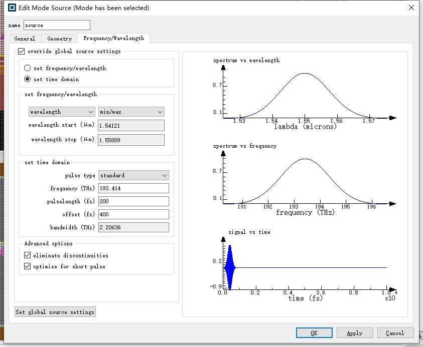
1.The plused light source setting in the FDTD
I set the light source to a pulsed light by set the source from "set frequency/wavelength" to "set time domain" in the settings of the mode source, and then set the parameters like the picture below.(It warned me that the image is failed to upload cause a XHR Transport error, but it seems ok on my page, so I'll state the parameters just to be on the safe side.)
pulse type:standrad
frequency:193.414
pulse length:200
pulse offset:400
2. The absorbed power calculated by FDTD
During this period of time, I have read the code of the analysis group for calculating the absorbed power and calculating the photogenerative carrier generation rate. My current understanding is that the photogenerative carrier generation rate obtained from the FDTD result analysis is a linear result for the power of the light source, that is, if the other parameters of the light source are unchanged and only the amplitude is adjusted, The photogenerative carrier generation rate and the optical power absorption rate are always the same because they are both normalized to the input amplitude.
3. The space charge shielding effect in the charge simulation
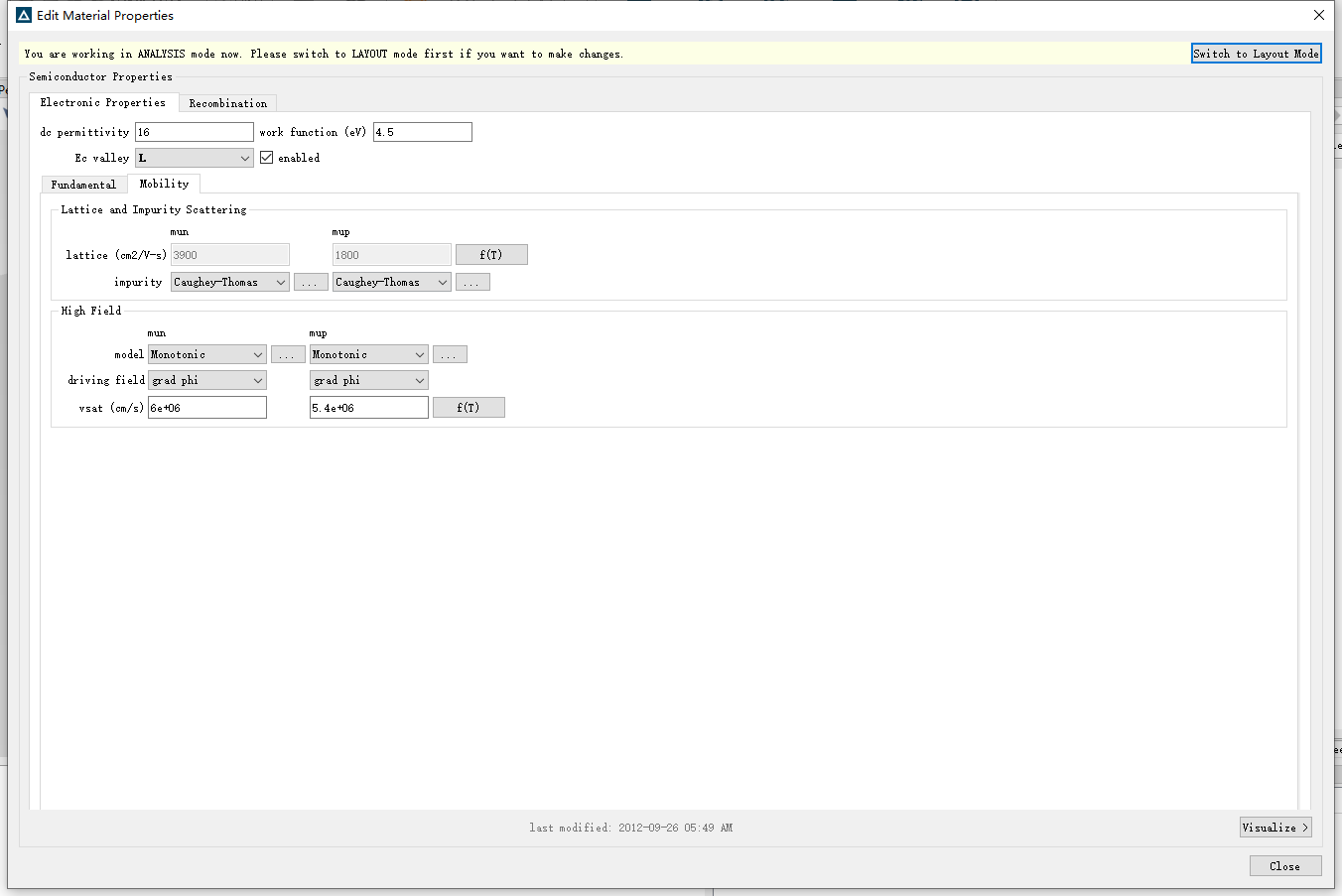
I mentioned before that I did not see the calculation formula of mobility in Charge solver. Later, I looked it up on the official website and found the description of the calculation process of Material mobility parameter from the introduction of Semiconductor Material Model Properties. Through reading this part, My understanding is that the space charge shielding effect caused by the injected carrier concentration has been taken into account, and this effect can be taken into account by setting a high field at the mobility setting in the material during the CHARGE simulation.
However, after opening the mobility model of this high field, when I changed the coefficient “a” in the photo-generated carrier source (according to my understanding, “a” is the average power of the light source, in unit W), the simulation often did not converge, indicating that the drift diffusion equation did not converge after 100 iterations, and I am now looking for the reason for the non-convergence.
https://optics.ansys.com/hc/en-us/articles/360034919113-Semiconductor-Material-Model-Properties
The above is my answer to your question, as well as my current understanding of this part. I hope to continue to communicate with you to discuss whether my understanding is correct.
Regards,
Mike
-
-
- You must be logged in to reply to this topic.


-
5934
-
1906
-
1420
-
1306
-
1021

© 2026 Copyright ANSYS, Inc. All rights reserved.


