We have an exciting announcement about badges coming in May 2025. Until then, we will temporarily stop issuing new badges for course completions and certifications. However, all completions will be recorded and fulfilled after May 2025.
Photonics

Photonics

Topics related to Lumerical and more.

simulating transmission within a phC waveguide – Lumerical FDTD

    • im1n21
      Subscriber

      Hi!

       I am trying to simulate the transmission spectra through a photonic crystal line defect waveguide of a specific geometry. My geometry looks like this:

      With the PML extending through the output waveguide, as suggested within this thread 

      /forum/forums/topic/simulating-photonic-crystal-waveguide-boundary-conditions-and-satbility/

      Because I am using a mode source over a wide frequency range, I am using multiple frequency dependent profiles to increase the accuracy over this range. I am injecting the mode profile of the input waveguide.

      To create my transmission spectra I have two DFT Monitors - one measuring the reflected power (behind the source) and one measuring transmission to the output waveguide. (See below for layout of monitors). 

      After simulating I get the result plots below but I am unsure about the results. I'm not entirely sure where power is being lost (I have been using a movie monitor to try and debug this, to no result) and additionally, these results have been very sensitive to small changes in input parameters.

      Any advice on how to carry out this type of simulation would be appreciated!! Thank you!!


    • Guilin Sun
      Ansys Employee

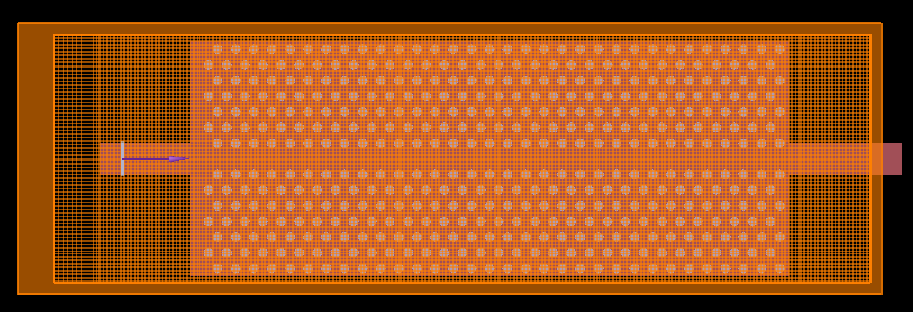
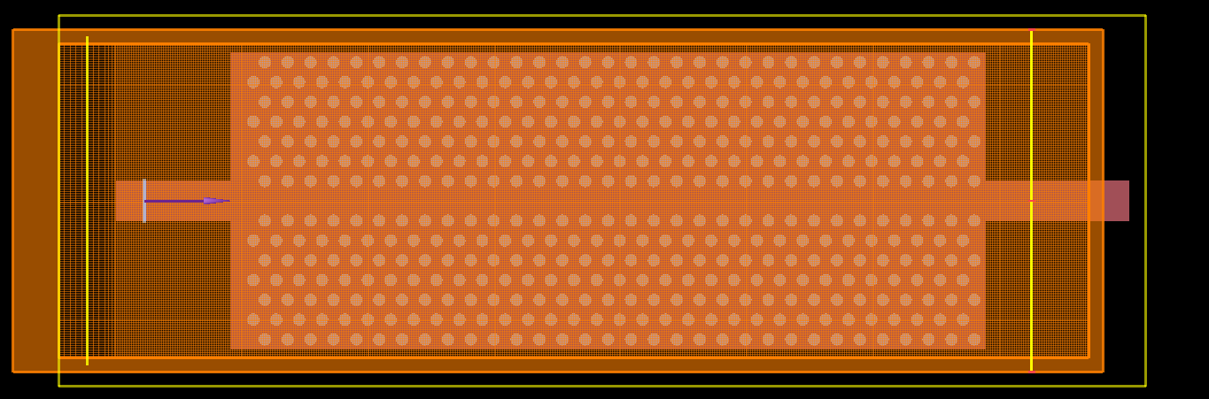
      I first suggest you to move the left PML closer to the cavity, eg, the input waveguide should penertate out the left PML. This will reduce reflection cased by the ending input waveguide, which may cause the uneven result.

      If you want to reduce memory, please shorten the distance between left and right PML BCs as only a small portion of the straight waveguides should work in your case.

      The loss  can arise from the sides of the photonics crystal waveguide because it has limited number of periods whereas in band structure simulation we assume infinite number of perioids. You can add some side power monitors to check the transmissions scattered out from the limited photonic crystal.  In addition, due to strong lattice resonance inside the photonic crystal, you may need to use smaller autoshutoff min provided the simulation time is long enough. You can use "checkpoint" to resume the simulation with reduced autoshutoff min and compare the results.

      https://optics.ansys.com/hc/en-us/articles/360046368573-Running-FDTD-simulations-from-the-design-environment

      so you do not need to simulate it from time zero when you reduce the autoshutoff min. Make sure you set the simulation time long enough and let the autoshutoff min to terminate the simulation. You can check the log file and see the percentage estimated from the simulation time. In all the times the percentage should be less than 100% at termination.

Viewing 1 reply thread
  • The topic ‘simulating transmission within a phC waveguide – Lumerical FDTD’ is closed to new replies.