-
-
March 5, 2024 at 6:00 pm
im1n21
SubscriberHi!
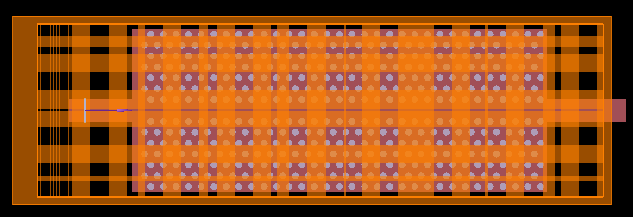
I am trying to simulate the transmission spectra through a photonic crystal line defect waveguide of a specific geometry. My geometry looks like this:

With the PML extending through the output waveguide, as suggested within this thread
/forum/forums/topic/simulating-photonic-crystal-waveguide-boundary-conditions-and-satbility/
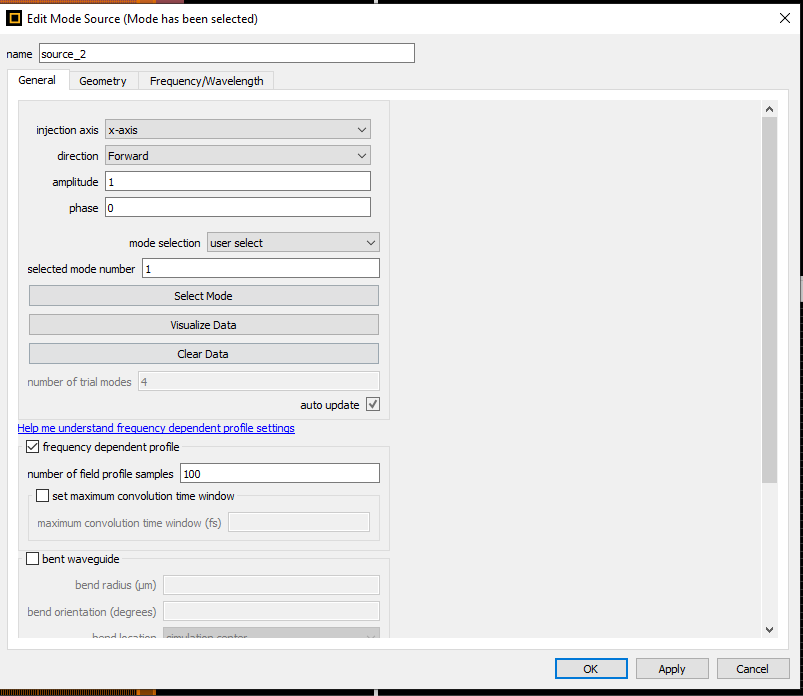
Because I am using a mode source over a wide frequency range, I am using multiple frequency dependent profiles to increase the accuracy over this range. I am injecting the mode profile of the input waveguide.

To create my transmission spectra I have two DFT Monitors - one measuring the reflected power (behind the source) and one measuring transmission to the output waveguide. (See below for layout of monitors).
After simulating I get the result plots below but I am unsure about the results. I'm not entirely sure where power is being lost (I have been using a movie monitor to try and debug this, to no result) and additionally, these results have been very sensitive to small changes in input parameters.
Any advice on how to carry out this type of simulation would be appreciated!! Thank you!!
-
March 5, 2024 at 7:57 pm
Guilin Sun
Ansys EmployeeNext time please waite for a few minutes if the post does not show after submission.
Your question in another post will be replied tomorrow.
-
- The topic ‘simulating transmission within a phC waveguide – Lumerical FDTD Duplicated’ is closed to new replies.


-
6254
-
1906
-
1457
-
1308
-
1022

© 2026 Copyright ANSYS, Inc. All rights reserved.


