
TAGGED: bending, explicit-dynamic, structure
-
-
May 27, 2021 at 9:36 am
amit.pandey
SubscriberHi,
I would like to simulate the bending or rather spherical deformation of a very thin silicon layer. I have a glass substrate at the bottom with a spherical cavity (concave) on which the silicon in placed. In the beginning only the four corners of the silicon layer will be in contact with the substrate. A tool with a convex surface presses down on the silicon surface and deforms it into spherical shape.
I tried to begin with a explicit dynamic simulation but the tool moves only when I specify a very high initial velocity and I get very high stress in the silicon.
Can someone describe how this simulation can be setup? I am mostly interested in the stress after the deformation process which I can later measure after the deformation with a Raman spectrometer.
Attached is an archive file for reference.
Any suggestions are most welcome.
Best regards,
Amit
PS: For the first simulation I am not simulating the adhesive layer between the silicon and the substrate. There is an additional process in between where the deformed silicon is held under force and the system is heated to complete the adhesive bonding process.
May 28, 2021 at 8:07 am1shan
Ansys EmployeeIt will be a better choice to use static structural instead of explicit dynamics since the inertia effects are negligible. Could you try doing this and see if it works. You could have a look at this three point bending tutorial to get an idea of the loading and boundary conditions https://www.youtube.com/watch?v=svE0ZW6QrrY. Since you don't have support rollers in your case you may use a bonded contact/no separation contact between the edges of silicon layer and glass substrate. Also, ANSYS staff are not allowed to download attachments. Please attach inline images next time to support your query.
Regards Ishan.
June 2, 2021 at 9:05 amSubscriber
Thank you for your response.
I tried doing what the video shows.
All my contacts are closed. I am using frictioneless contacts between the components.
However, I still believe that the corners of the silicon chip in contact to the bottom substrate will try to move up when the tool presses against it. So, I guess bonded/no separation might generate additional stress.
Also, all the bodies in my CAD are solid bodies, I am not sure if that will make a difference in the end but I am not able to converge on a solution.
i see some penetration between the substrate and the silicon which I tried to rectify by using Normal Lagrange formulation but then the solution does not converge because some element become highly distorted.
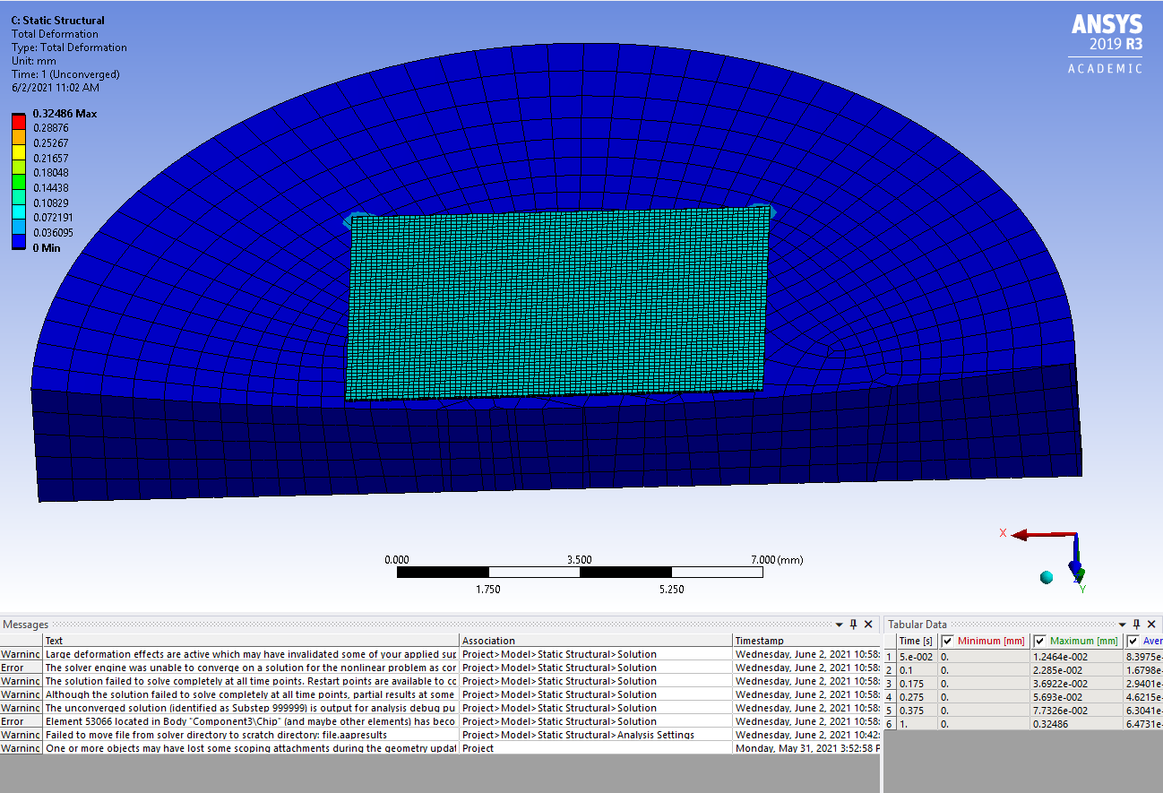
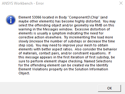
June 2, 2021 at 1:03 pmAnsys EmployeeHave you turned large deflection under Analysis settings as 'ON' ? Also, if its a thin sheet a better option would be to use a 2D mesh (or you will need more than one element across the thickness). Also, If you are not interested in the deformations of the lower glass substrate define its stiffness behavior(under geometry) as rigid. The solver will not mesh the rigid body saving unnecessary expense. Have you used a bonded contact at the 4 corners? Looks like the geometry is symmetric. If so just model 1/4th of the geometry and use the symmetry object - https://www.youtube.com/watch?v=RETzoXbbwBA. You could see which elements are distorted by setting a number to 'element violations' under solution information.
Regards Ishan.
June 7, 2021 at 11:28 amSubscriber
I have now simplified my model to a base block and sphere that you can see here in the image below:
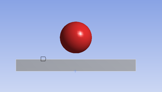
I set the contact condition as frictionless.
The block is fixed supported on the 5 outer faces (expect the one in contact with the sphere).
The sphere has a displacement boundary condition of 5mm in the Y direction.
With these settings I see the sphere deforms the block:
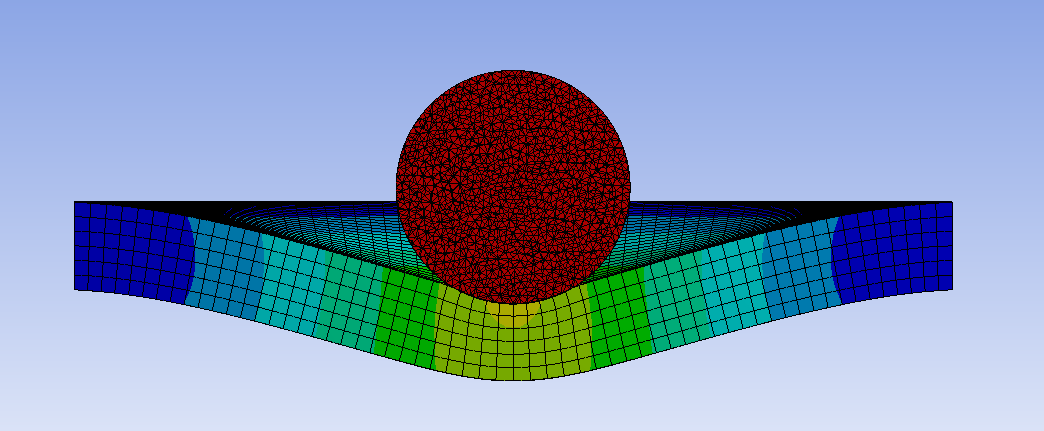
my aim is to deform the sphere (or whatever component is on top of the block, maybe a silicon chip later). Then, I tried to increase the Young's modulus of the block material to be greater than that of the sphere. And I also tried to change the block to be a rigid body and apply Joint in the "connections" settings.
With the joints settings and the rigid behavior of the block I see that the sphere just moves though the block for 5mm and does not deform. I also change the "advanced: formulation" setting in the contacts to pure penalty and augmented lagrange but there is no deformation, only the sphere passes through the block.
my ultimate goal is to make the sphere deformed when it comes into contact with the block but what happens is the block deforms.
Could you please point out, what I am doing wrong?
Best regards Amit
June 8, 2021 at 1:19 ampeteroznewman
SubscriberHello Amit I liked 's suggestion to do 1/4 symmetry on the silicon chip. That leaves a single DOF that is taken care of by frictional contact between the chip and the base with the spherical dish and the chip and the sphere. I agree that the silicon chip should be shell elements meshed on a square surface. I agree that the sphere and base should be rigid bodies. Note that only the silicon chip can have symmetry boundary conditions, the rigid bodies don't get that treatment. That model should solve without too much difficulty. Attach a .wbpz file and I will help get that model working.
June 8, 2021 at 6:52 amSubscriberThank you for your response and your effort to help get the model working. I have attached the archive for the model with the concave substrate and silicon chip.
When I set the substrate as a rigid body, the silicon just moves into the substrate and there is not curved deformation which I expect to happen.
With best regards Amit
June 8, 2021 at 5:59 pmSubscriberHello Amit The archive did not include the Silicon+lens+tool.stp file that I need to create a 1/4 symmetry model.
Please put check the box to include outside files and that should end up in the archive. Then attach a fresh copy.
June 9, 2021 at 7:31 amSubscriberHello Peter
Attached is the new archive file. I have archived everything including the results to make sure it work, however it was not solved.
In the geometry, there are three components. Concave glass dish at the bottom (serves as mould for the chip curving process), a thin silicon chip and a tool on top to press the chip into the mould.
I am not too concerned about the pressing tool so it can be suppressed. I am more concerned about the stress in the silicon after it has been deformed. There is an intermediary process in the bonding of the chip to the mold by adhesive and heating it which will produce additional stress as it cools down but I think I am getting ahead of myself.
Thank you again for your offer to help..
With best regards Amit
June 9, 2021 at 12:02 pmSubscriberHello Amit
June 9, 2021 at 2:49 pmSubscriberHello Peter
Thank you for the help.
I will try to tweak the simulation with friction coefficients that would better represent my system. I would measure the stress and then let you know how that turns out to be.
Thanks a lot for the help.
With best regards Amit
August 3, 2021 at 9:25 amSubscriber
I have a new challenge in the simulations.
I want to simulate the bonding process of the silicon chip to the glass substrate after it has curved. In this step an adhesive layer is already on the silicon chip when it is being pressed into the form and then the system is heated to harden the adhesive. When the system cools down, there will be stresses in the chip in addition to the stress due to the curve formation.
I had an idea of doing this using the element birth and death, however, keeping the adhesive layer dead does not do justice because then the silicon will come into contact with the substrate but I want the adhesive film to be the intermediate layer between silicon and glass substrate.
Is there a simpler way to do this?
With regards Amit
August 3, 2021 at 12:23 pmSubscriberTry contact with Keyop(12)=5. Make a small test model to confirm that this works the way you want.
The contact can be open at the start of the simulation, and as the pressure pushes the silicon chip down, the contact closes and holds the chip from that time onward.
Regards Peter
Viewing 12 reply threads- The topic ‘Simulating the bending/deforming of a flat, thin silicon layer into a spherical geometry’ is closed to new replies.
Innovation Space Trending discussions
 Top Contributors
-
peteroznewman
 5794
5794 -
scabo
 1906
1906 -
Dennis Chen
 1419
1419 -
javat33489
 1305
1305 -
Shyam Prasad V Atri
1021
Top Rated Tags
© 2026 Copyright ANSYS, Inc. All rights reserved.
Ansys does not support the usage of unauthorized Ansys software. Please visit www.ansys.com to obtain an official distribution.
-


