

-
-
June 1, 2021 at 2:57 pm
cqtavee
SubscriberHi All
I'm simulating an edge coupler similar as Edge coupler – Lumerical Support
I download the package and find the codes of building the structures in the file Edge_Coupler_No_Substrate.lms
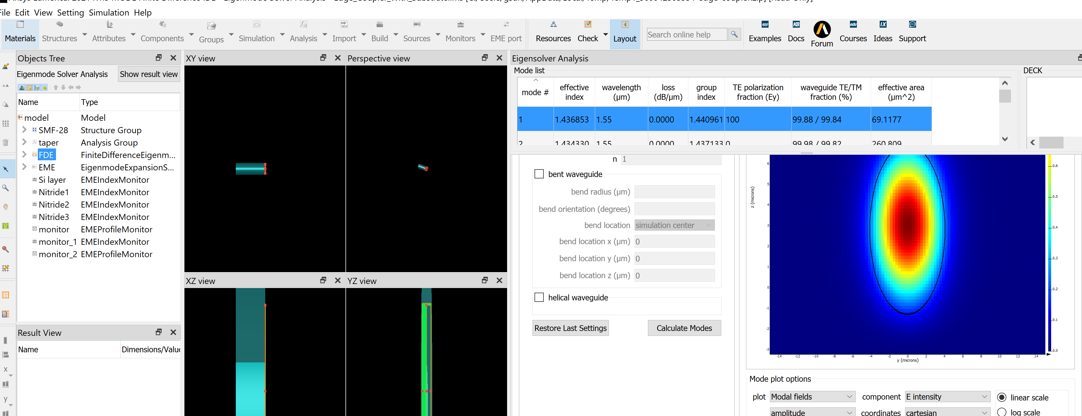
I copied down the scripts and added the same SMF-28 fibre by codes. But I cannot get the same mode profile as the example project. I'm very sure I'm using the same parameters like the example. The first one is my result, and the second is the mode profile from the example file.
June 1, 2021 at 10:21 pmGuilin Sun
Ansys EmployeeI am not sure what script you copied for what purpose. If you just want to investigate the modes for SMF fiber, simply enable FDE, disable the taper, and you will be able to get the mode as follows:
 Since we are not allowed to download customer files, please copy and paste here and explain what do you expect the script file to accomplish.
The result you gave shows it has circular and ridge waveguide together. Please check the geometry carefully.
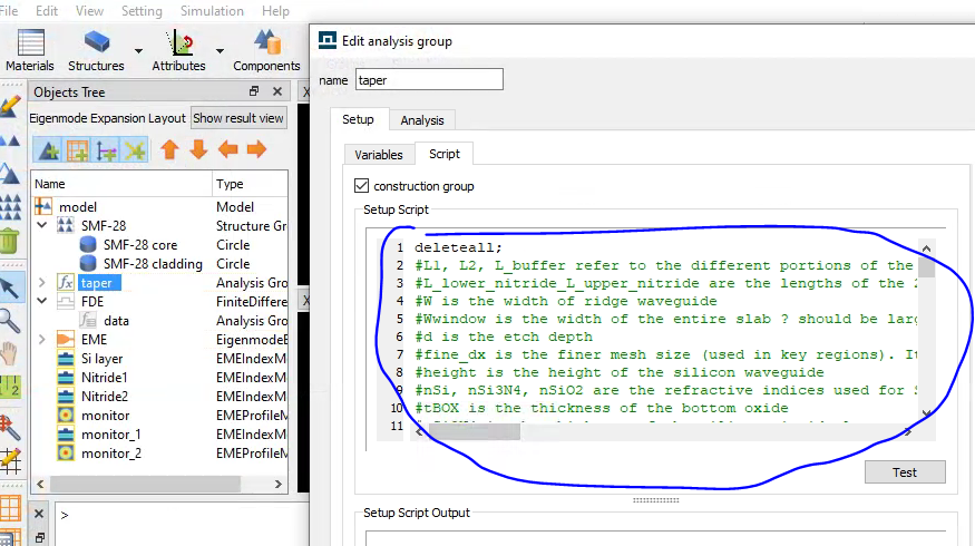
June 2, 2021 at 4:03 amSubscriberHi! Below are my codes.
deleteall;#L1, L2, L_buffer refer to the different portions of the Si waveguide and are the lengths of the untapered input section, the tapered section, and the untapered end section, respectively
#L_lower_nitride_L_upper_nitride are the lengths of the 2 silicon nitride layers
#W is the width of ridge waveguide
#Wwindow is the width of the entire slab ? should be larger than simulation region
#d is the etch depth
#fine_dx is the finer mesh size (used in key regions). It controls dy and dz around the silicon waveguide, and dz in the nitride layers. It should never be larger than the thickness of the nitride layers or the conformal meshing will not work.
#height is the height of the silicon waveguide
#nSi, nSi3N4, nSiO2 are the refractive indices used for Si, Si3N4 and SiO2 (note that these could be changed to use a model from the database, but it does speed up the calculation to use a lossless dielectric and these materials have negligible loss at 1550nm)
#tBOX is the thickness of the bottom oxide
#tSi3N4 is the thickness of the silicon nitride layers
#tSiO2_1,tSiO2_2,tSiO2_3, tSiO2_4 are the thicknesses of the SiO2 layers from the top of the BOX to the bottom of the first nitride layer, between the first and second nitride layers, between the second and third nitride layers and from the upper nitride layer to the top of the waveguide.
#tw1 and tw2 are the widths of the input and output silicon waveguides, respectively
deleteall;
#input parameters
L1=50e-6;
nSiO2=1.444;
tSi3N4=0.02e-6;
tSiO2_1=2.72e-6;
tSiO2_2=2.72e-6;
tSiO2_3=2.72e-6;
tw1=0.15e-6;
tw3=0.27e-6;
L2=405e-6;
L_buffer=5e-6;
L_lower_nitride=400e-6;
L_upper_nitride=50e-6;
W=14.15e-6;
Wwindow=50e-6;
d=6.5e-6;
height=0.22e-6;
nSi=3.476;
nSi3N4=2.016;
tBOX=15e-6;
fine_dx=0.02e-6;
include_input_buffer=0;
L_middle_nitride=200e-6;
tSiO2_4=2.72e-6;
L_buffer_in = L_buffer;
if(!include_input_buffer) {
L_buffer_in = 0;
}
n_fiber_cladding=1.434816;
n_fiber_core=1.44;
radius_fiber_core=4.1e-6;
#Add fiber cladding
addcircle;set('name','fiber cladding');
set('x',-50e-6);set('z span',100e-6);
set('radius',20e-6);
set('material','June 2, 2021 at 4:07 amSubscriberHi! The codes I copied are from here:
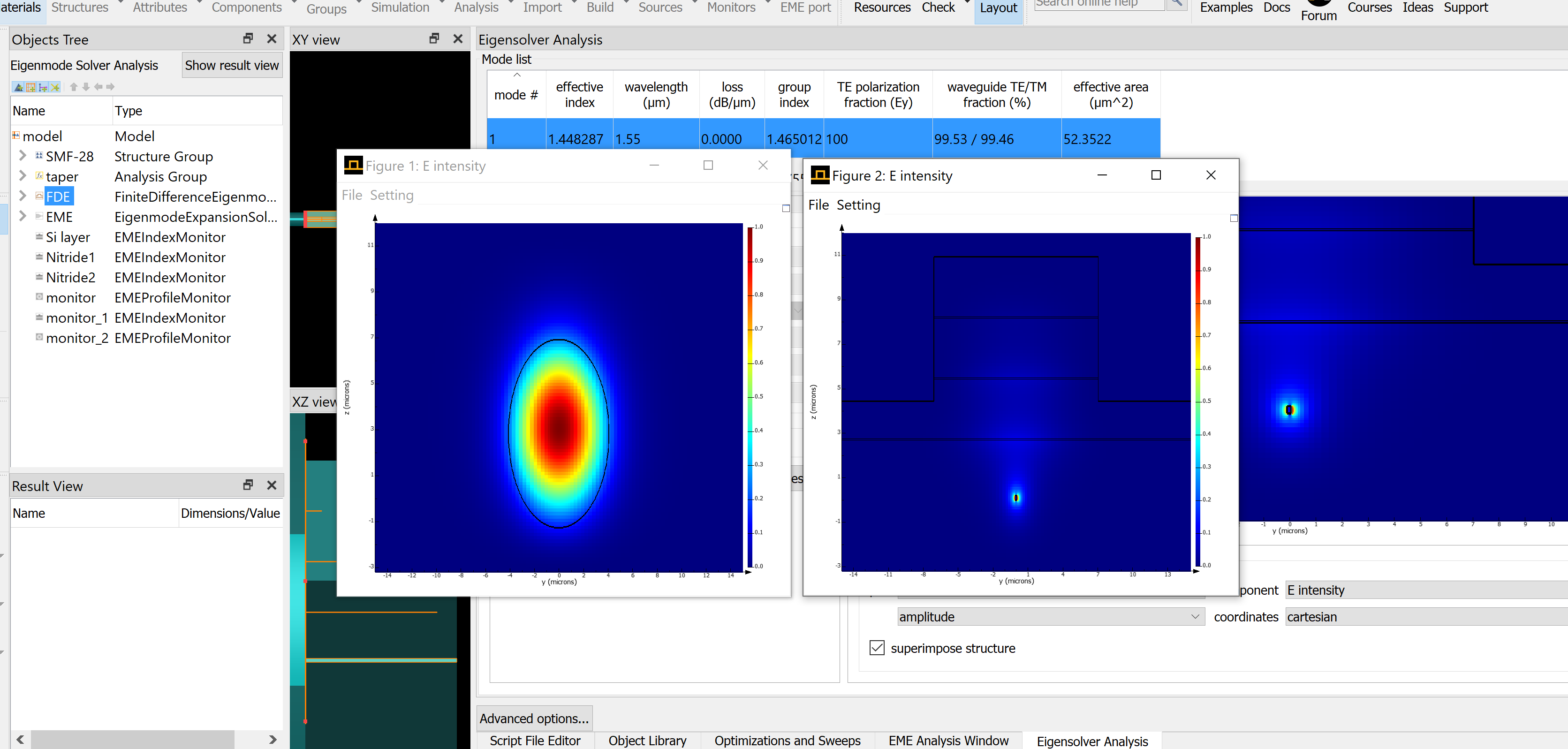
 The main body is unchanged. I just add some lines to add fiber and FDE simulation area. But the result (mode profile at x=0) of my project is very different from the downloaded one although they are using the same parameter values.
Thank you so much!
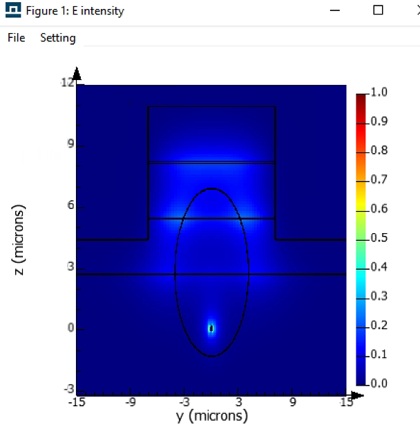
June 4, 2021 at 11:25 pmAnsys EmployeeHi, I run your code and can duplicate your result, except the multiplier issue mentioned somewhere else.
FDE solver somehow interpolates the refractive index of the fiber and the taper, this is why we got riedge waveguide profile + fiber. If you only want to analyze mode properties using FDE, a simple way is to modify the x position of FDE:
for fiber, set x=-1um; for taper set x=1um. With those modifications I got two results for the two waveguides:fiber and the taper.
June 8, 2021 at 8:11 amSubscriberHi
Yes, you are right, that's a good idea to view the mode profiles at different x position. BTW, I have solved the mesh multiplier issue.
I can first add FDE and then select the mesh to set the multiplier setting.
addmesh;set("x min",-L_buffer_in);
set("x max",L1+L2+L_buffer);
set("y",0);
set("y span",Wwindow);
set("z min",-2*tBOX);
set("z max",-tBOX);
set("override x mesh",false);
set("override y mesh",false);
set("override z mesh",true);
set("name","Si substrate override");
addfde;
select("Si substrate override");
set("set mesh multiplier",true);
set("z mesh multiplier",4);
June 8, 2021 at 3:42 pmAnsys EmployeeThank you for the update! you are right that in general, we should first add the solver, then the override mesh, which can give a better guess of the default mesh size in the override region.
Viewing 6 reply threads- The topic ‘Same codes, different result? Edge coupler design with MODE FDE’ is closed to new replies.
Ansys Innovation Space Trending discussions
 Top Contributors
-
peteroznewman
 2878
2878 -
javat33489
 970
970 -
Shyam Prasad V Atri
 852
852 -
ashishkumar.gupta
 599
599 -
sharifulgit24
591
Top Rated Tags
© 2025 Copyright ANSYS, Inc. All rights reserved.
Ansys does not support the usage of unauthorized Ansys software. Please visit www.ansys.com to obtain an official distribution.
-


The Ansys Learning Forum is a public forum. You are prohibited from providing (i) information that is confidential to You, your employer, or any third party, (ii) Personal Data or individually identifiable health information, (iii) any information that is U.S. Government Classified, Controlled Unclassified Information, International Traffic in Arms Regulators (ITAR) or Export Administration Regulators (EAR) controlled or otherwise have been determined by the United States Government or by a foreign government to require protection against unauthorized disclosure for reasons of national security, or (iv) topics or information restricted by the People's Republic of China data protection and privacy laws.
