-
-
May 22, 2024 at 7:40 pm
pnair
SubscriberHello,
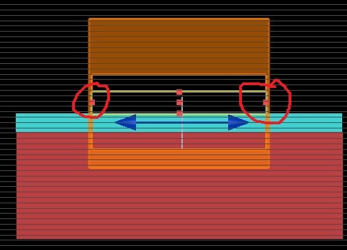
I have a question related to the placement of side monitors on the thin film. I am using box of monitors with 6th monitor is deactivated as it is on the substrate. But, I know the top monitor should be placed at a distance of greater than or equal to half of the emission wavelength(From lumerical resources). For example in my simulations, it is around 1540nm wavelength, So, I have placed top monitor around 0.85um from the FDTD boundaries on the top. So, i would like to know this rule is applicable for side placement of side monitors from side FDTD boundaries. Please find the attached figures for the reference. I have tried different cases where the side monitors are 1) 1um from FDTD region, 2) in the FDTD region, 3) 2.5 um from FDTD boundaries. I got almost similar farfield patterns in the case with slight difference in the intensity values.
Could you please suggest me further regarding this about how to validate the distance from the FDTD boundary regions for the side monitors as shown in the above pictures?
-
May 23, 2024 at 6:37 pm
Amrita Pati
Ansys EmployeeHi Prabha,
Keeping the monitor half a wavelength away from the PML is not based on an exact equation but more of a rule of thumb for most simulations. I will recommend placing it about 1 um away. In the 2nd screenshot, it looks like the monitor is in the PML, so I am not even sure if it is recording the fields. If you do not see any difference between the 1 um and 2.5 um, then I will recommend using the first as you can same time and resources simulating a smaller simulation domian.
Regards,
Amrita
-
- The topic ‘Regarding the Farfield simulations and placement of monitors’ is closed to new replies.


-
5664
-
1890
-
1419
-
1304
-
1021

© 2026 Copyright ANSYS, Inc. All rights reserved.


