We have an exciting announcement about badges coming in May 2025. Until then, we will temporarily stop issuing new badges for course completions and certifications. However, all completions will be recorded and fulfilled after May 2025.
Photonics

Photonics

Topics related to Lumerical and more.

RCWA, interfaces

TAGGED: ,

    • Ekaterina Pshenay-Severin
      Subscriber

      Hi, could you help me understand how to define interfaces in the RCWA object? I'm simulating a Si grating on a Si substrate with a SiO2 superstrate. I'm using "interference reference positions". Currently, I only need one interface at each point, but the discretization of the index is incorrect. Could you explain how I should define the interfaces in this case?

    • Amrita Pati
      Ansys Employee

      Hi Ekaterina,

      The "interface reference positions" are based on the maximum and minimum of each object in the simulation. This is why you see multiple points at the same location as the maximum of one object is same as the minimum of a different object. You can enable only one of these points (same locations) to be selected as the layer interface in the simulation. For example max(substrate) then min(etch) then max(etch).

      Please let me know if you have any further questions.

      Regards,
      Amrita

    • Ekaterina Pshenay-Severin
      Subscriber


      Dear Amrita,

      Thank you a lot for the response. This is what I am doing. But the first slab starts almost at -0.4 µm though the interface point is at -0.5 µm. 

      The last interface is at 0.72 µm but in the index plot the last point is at 0.6 µm. Why?

      Regards,

      Ekaterina


    • Amrita Pati
      Ansys Employee

      Hi Ekaterina,

      Thank you for sharing more information. Is the refractive index plot consistent with the geometry you have defined?

      Regards,
      Amrita

    • Ekaterina Pshenay-Severin
      Subscriber

      Dear Amrita,

      the refractive index plot is not consistent with the geometry. WG MIN is at 0 µm, and the total WG height (WG MAX = etched MAX) is 220 nm.

      Regards, Ekaterina.

    • Amrita Pati
      Ansys Employee

      Hi Ekaterina,

      Thank you for providing more details. Would you be able to share a screenshot of the code you have used to set up the structure group? The inconsistent index plot might be because of an incorrect setup.

      Regards,
      Amrita

    • Ekaterina Pshenay-Severin
      Subscriber

      Hi Amrita,

      here it is

      thank you!


    • Amrita Pati
      Ansys Employee

      Hi Ekaterina,

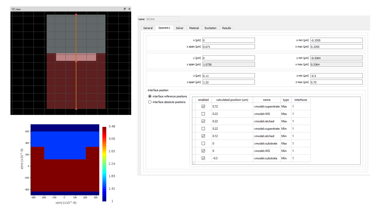
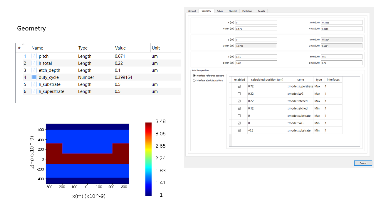
      I tested your code. In this case, you should include, one interface at 0 microns, second at 0.12 microns and third at 0.22 microns. The substrate and superstrate should not be included as interfaces. But the simulation region should extend into the substrate and the superstrate so that the simulation knows which medium the light is incident from and which medium it is transmitted to. The schematic is shown below:


      That being said, as you said the index results provided by RCWA seem to be inconsistent. The co-ordinates seem to be shifting depending upon the location of the simulation region which is unusual whereas the FDTD index monitor is returning the expected results as shown below. This might be due to a bug. I will investigate it further and get back to you as soon as I can.

      Regards,
      Amrita

    • paolo.biagioni
      Subscriber

      I am experiencing the exact same problem, the index monitor embedded in the RCWA software seems to provide inconsistent results... however, the electromagnetic results seem consistent with the nominal thicknesses... can you confirm that we can trust 100% the nominal thicknesses that we input in the layout and that the bug regards only the index output?

      • paolo.biagioni
        Subscriber

        Dear Amrita, dear support staff,

        is there any further development regarding the issue discussed in this thread? In particular, can you confirm that we can trust 100% the nominal thicknesses that we input in the layout and that the bug regards only the index output?

        Thanks, Paolo

    • Amrita Pati
      Ansys Employee

      Hi Paolo,

      Sorry I missed this post. In cases like this you can always create a new one referencing the old one. I had spoken to the R&D team on this. The issue here is because of an artifact of the visualization. There is only one data point for each layer in the simulation in the index data, placed at the position (along the propagation direction) in the middle of the layer. This means there is only one point for the substrate/cladding in the index data. The visualization then fills in half of the area between the substrate/cladding layer with the colors from the top/bottom layer in the visualization, creating this issue where the thicknesses looks different. I was told that the correct way to visualize the index data is to use view the transverse axes in the graph/visualizer. For example, if the propagation is z, then we should visualize the x and y axes. We should visualize the index in the xy plane, and the z-axis in the visualizer should be Slice. This means you view the xy plane for each value of z. 

      This artifact does not affect the results of your RCWA simulation.

      Regards,
      Amrita


Viewing 9 reply threads
  • The topic ‘RCWA, interfaces’ is closed to new replies.