TAGGED: mechanical, odb-design, trace-mapping
-
-
February 17, 2022 at 8:56 pm
blackra1n
SubscriberHello,
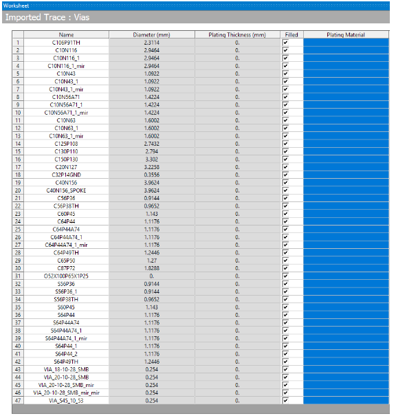
I have a question about trace mapping. When I imported trace in Ansys mechanical, plating thickness is always 0. I know I can change it by unchecking fill box, but I thought Ansys should be able to read it automatically. In general, can some one explain more about plating thickness column.
Thank you,
(there are lots of ODB++ file online. No matter which one you try, plating thickness is always 0.)
February 21, 2022 at 3:35 pmGary Stofan
Ansys EmployeeIt is the plating thickness of a via if it is unfilled.
Trace Mapping in Mechanical (ansys.com)
Plating Thickness This field displays the thickness of the interior wall of the via that is not filled. Only applicable when via is hollow (not filled).
Filled Check and/or uncheck this fill to indicate whether the vias is filled or hollow.
This field is always 0 in all imports I have seen.
Viewing 1 reply thread- The topic ‘Plating Thickness – Trace Mapping’ is closed to new replies.
Ansys Innovation Space Trending discussions
 Top Contributors
-
peteroznewman
 3832
3832 -
scabo
 1414
1414 -
Dennis Chen
 1193
1193 -
javat33489
 1100
1100 -
Shyam Prasad V Atri
1015
Top Rated Tags
© 2025 Copyright ANSYS, Inc. All rights reserved.
Ansys does not support the usage of unauthorized Ansys software. Please visit www.ansys.com to obtain an official distribution.
-


The Ansys Learning Forum is a public forum. You are prohibited from providing (i) information that is confidential to You, your employer, or any third party, (ii) Personal Data or individually identifiable health information, (iii) any information that is U.S. Government Classified, Controlled Unclassified Information, International Traffic in Arms Regulators (ITAR) or Export Administration Regulators (EAR) controlled or otherwise have been determined by the United States Government or by a foreign government to require protection against unauthorized disclosure for reasons of national security, or (iv) topics or information restricted by the People's Republic of China data protection and privacy laws.