TAGGED: 3DFDTD, Bloch, convergence, plane-wave
-
-
October 25, 2023 at 10:03 am
Erik M
SubscriberI would like to compute the transmission of a wave travelling though an infinetly wide waveguide slab. The geometry consists of a 220 nm thick waveguide slab in which the wave is injected, followed by a 130 nm deep step. The angle is varied from 0 to 85 degrees. The source wavelength is fixed to 1550 nm.
To simulate an infinitely wide slab, I use Bloch periodic boundary conditions (in y) in combination with a plane wave source (PlaneSource, injected in x). In my simulation, I find that the Autoshutoff criterium is not reached, because some light is reflected back and forth between the periodic boundaries. As a result, the energy in the system decays only slowly (see image below). In addition, the pulse seems to become wider as it propagates through the slab. These problems are bigger for larger incidence angles.
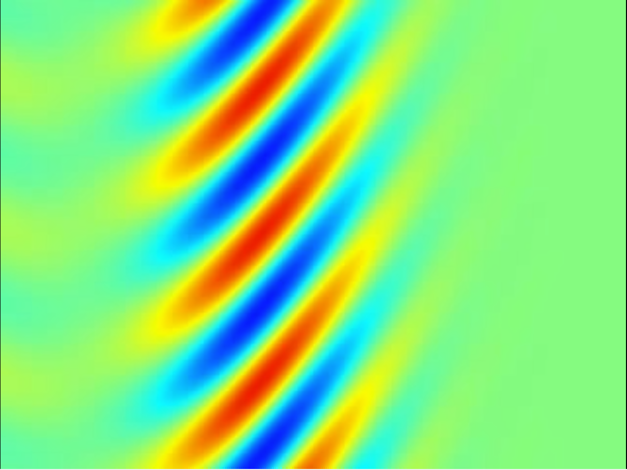
y-component of field with incidence angle = 60 degrees shortly after injection of the pulse. No height step, waveguide thickness is 220 nm.
y-component of field with incidence angle = 60 degrees when the pulse has passed through the simulation domain. No height step, waveguide thickness is 220 nm.Is this an artefact of the plane wave source? And if yes, what can I do minimise this effect and/or correct for it in a transmission measurement?
Many thanks,
ErikBelow is sample code (lsf) that can be used to recreate my problem. Use d2_z = 220e-9; for the simulation without the height step and d2_z = 90e-9; for a simulation with a step. The angle of incidence can be varied via deg_angle.
"""
switchtolayout;
selectall;
delete;
### Variables
size_x = 8000e-9;
size_y = 10000e-9;
size_fdtd_x = 4000e-9;
size_fdtd_y = 2000e-9;
size_fdtd_z = 1500e-9;
x_offset = 0;
deg_angle = -45;
z_min = 0;
d1_z = 220e-9; # height
d2_z = 220e-9;
center_wavelength = 1550e-9;
mesh_accuracy = 5;
### Main
poly_name = "rectangle";
addrect();
set('name', poly_name + "_1");
set('x min',-size_x/2+x_offset);
set('x max',0+x_offset);
set('y min',-size_y/2);
set('y max',size_y/2);
set('z min',0);
set('z max',d1_z);
set('material', 'Si (Silicon) - Palik');
addrect();
set('name', poly_name + "_2");
set('x min',0+x_offset);
set('x max',size_x/2+x_offset);
set('y min',-size_y/2);
set('y max',size_y/2);
set('z min',0);
set('z max',d2_z);
set('material', 'Si (Silicon) - Palik');
## FDTD
addfdtd();
set('mesh accuracy',mesh_accuracy);
set('dimension','3D');
set('x min',-size_fdtd_x/2);
set('x max',size_fdtd_x/2);
set('y min',-size_fdtd_y/2);
set('y max',size_fdtd_y/2);
set('z min',-size_fdtd_z/2.0+200e-9);
set('z max',size_fdtd_z/2.0+200e-9);
set('y min bc','Bloch');
set('index',1.44);
set('pml profile',3); # steep angle PML profile
# SOURCE
addplane();
set('direction','Forward');
set('injection axis','x-axis');
set('y min',-size_y/2);
set('y max',size_y/2);
set('z min',0);
set('z max',d1_z);
set('x',-size_fdtd_x/2+0.5e-6);
set('center wavelength',center_wavelength);
set('wavelength span',0);
set('angle theta',deg_angle);
# MOVIE MONITORS
addmovie();
set('name','Movie_top_intensity');
set('monitor type','2D Z-normal');
set('x min',-size_fdtd_x/2);
set('x max',size_fdtd_x/2);
set('y min',-size_fdtd_y/2);
set('y max',size_fdtd_y/2);
set('z',d1_z/2);
addmovie();
set('name','Movie_top_Ey');
set('monitor type','2D Z-normal');
set('x min',-size_fdtd_x/2);
set('x max',size_fdtd_x/2);
set('y min',-size_fdtd_y/2);
set('y max',size_fdtd_y/2);
set('z',d1_z/2);
set('field component','Ey');
set('TM field component','Hy');
set('TE field component','Ey');
addmovie();
set('name','Movie_side_intensity');
set('monitor type','2D Y-normal');
set('x min',-size_fdtd_x/2);
set('x max',size_fdtd_x/2);
set('y',0);
set('z min',-size_fdtd_z/2.0+200e-9);
set('z max',size_fdtd_z/2.0+200e-9);
addmovie();
set('name','Movie_side_Ey');
set('monitor type','2D Y-normal');
set('x min',-size_fdtd_x/2);
set('x max',size_fdtd_x/2);
set('y',0);
set('z min',-size_fdtd_z/2.0+200e-9);
set('z max',size_fdtd_z/2.0+200e-9);
set('field component','Ey');
set('TM field component','Hy');
set('TE field component','Ey');
"""
-
October 25, 2023 at 5:28 pm
Amrita Pati
Ansys EmployeeHi Erik,
Thanks for the detailed information and the code. Let me look at this and get back to you very soon.
Regards,
Amrita -
October 25, 2023 at 10:26 pm
Amrita Pati
Ansys EmployeeHi Erik,
I had a look at your simulation. I do not see any issue with the setup of the Bloch Boundary conditions. But the problem is that Plane Waves or Gaussian beams are used in free-space optics i. e. they should be injected in homogenous medium. Once it has been injected into a homogenous medium, you can look at how much of it is transmitted/reflected by structures or how much is coupled into a waveguide. But it should not be injected into structures directly or you will most likely see injection error.
For ex. if you look at the screenshot below, you can see that there is some field intensity behind the source as it is being injected, which is not physical:
This also happens when theta = 0 with periodic boundary conditions. For theta = 0, I put a DFT monitor behind the source, you can see that there is a large amount of reflection which, again, should not happen:
Let me know if you have any questions.
Regards,
Amrita -
October 26, 2023 at 7:26 am
Erik M
SubscriberDear Amrita,
Thank you very much for your answer and reproducing my simulation.
You wrote that a plane wave source should not be used to inject a mode into a slab waveguide. My follow-up questions are:
- How would you recommend to inject a mode into a slab waveguide with Bloch periodic boundary conditions? To the best of my knowledge, the mode source does not support Bloch boundary conditions.
- If it is not possible to perform a simulation as described above, how would you set up a simulation to measure the transmission through an (infinitely) wide waveguide slab containing a height discontinuity?
I am looking forward to your thoughts.
Regards,
Erik -
October 27, 2023 at 5:36 pm
Amrita Pati
Ansys EmployeeHi Erik,
That is correct, Periodic and Bloch Boundaries are used with non-diffracting plane waves to approximate their infinite curvature.
About your second point, I will think about it. Typlically, I would use mode source with PML boundaries, Bloch/Periodic are not required. But since this this is an infinitely wide slab waveguide, I am not sure if this will yield accurately results. Typically, when we inject a mode source the fields should decay sufficiently enough at the edges of the simulation domain (as they are localized 2D modes in a waveguide). I have seen situations where results become inaccurate when there is a large magnitude of the fields at the edges (which will happen here). But I will spend some time on this and get back to you.
In the meantime, would you be able to explain what is the motive behind the simulation? For instance, are you trying to mimic experimental conditions, or validate a theoretical framework? I am asking because it might help us identify what options we have. Thank you!
Regards,
Amrita -
October 30, 2023 at 7:06 am
Erik M
SubscriberHi Amrita,
Thank you for your reply. I can comment on the goal of my simulations.
I would like to understand:
- how a wavefront of a mode confined in z behaves when it hits an interface; and
- what the errors are when this is simulated in 2D using an effective refractive index approximation.
I am particularly interested in the transmission power, phase shift, and out-scattering losses in the 3D simulation (compared to the 2D simulation) as function of incidence angle (0–85 degrees).
To generalise the results, I would like to do this simulation in an infinitely wide waveguide slab. This would help me (among other things) to decide in what conditions I can use 2D simulations (instead of 3D) and estimate the introduced errors.
Regards,
Erik -
November 17, 2023 at 1:36 pm
Erik M
SubscriberHi Amrita,
Would you have a suggestion how to tackle the questions/problems outlined in my posts above? Many thanks for your ideas and suggestions!
Regards,
Erik -
November 17, 2023 at 9:57 pm
Amrita Pati
Ansys EmployeeHi Erik,
Sorry about this, I did discuss your simulation with my colleague a few days back, but I didn't have time to test these suggestions myself so, I hadn't posted my reply.
In our opinion, the results for example the transmisson spectrum should't change from 0 to 85 deg, as the slab is infinite along the y-direction. So, in our opinion you should change the orientation of the structure and perform a single 2D simulation. The infinite direction "y" should now be along the "z"-direction.
But we also think that it would be interesting to do 3D simulation as well, and the results should be identical or very close in our opinion. For a 3D simulation we would also ask you to inject a mode source. Then in mode slection choose "user select" followed by "Select mode". The eigenmode solver will pop-up. Then go to its boundary conditions tab, override the default boundaries and change the y boundary to Bloch.
Let me know if you have questions.
Regards,
Amrita-
November 23, 2023 at 12:41 pm
Erik M
SubscriberDear Amrita,
Thank you for coming back to this. For a slab waveguide, I also do not expect a dependence of the transmission on the incident angle. However, I will introduce a height discontinuity in the slab waveguide, which in turn, leads to a dependence on the incident angle. (For instance, I expect to see total internal reflection above certain indicent angles.)
I tried to implement your suggestion in the post above. I used the script in my first post to build the geometry and exchanged the plane wave source for a mode source. However, I am not able to select the bloch boundary condtions. Moreover, I suspect that setting the boundary conditions for the source only will not change how the boundary conditions are applied to the propagating wave through the waveguide.
What am I missing here?
Regards,
Erik
-
-
- The topic ‘Plane wave and Bloch boundary conditions in slab waveguide’ is closed to new replies.
- Import material .txt file with script
- Errors Running Ring Modulator Example on Cluster
- Absorption cross-section of AuNR excited by prism-based TIR
- How to measure transmission coefficients on a given plane .
- TE Polarization Fraction + Waveguide TE/TM Fraction
- Edge Coupler EME Example Issue
- Lumerical Python API Topology Optimization Error 2025 R1
- 2D inverse design grating coupler
- FDE : Simulation waveguides with electrodes
- Loss of lithium niobate phase modulator
-
2337
-
925
-
599
-
591
-
527
© 2025 Copyright ANSYS, Inc. All rights reserved.