-
-
April 27, 2021 at 3:42 pm
bsr
SubscriberHi,- What is the right approach for analyzing i.e. evaluating parasitics of the pcb design with Altium? I am using ODB++ files of Altium, importing in SiWave and then exporting using Q3D extractor?
- How do I ensure that the exported design for Q3D analysis has hollow vias? Under export options, this setting is unchecked "100% via fill (overrides per-padstack plating ratio)". Just to give more context, I can only choose top and bottom faces of the vias within Electromangnetic suite while assigning excitation. If hollow vias are available, then I might be able to choose the inner cylinder of the via. How can I validate whether a hollow or filled via is exported using Q3D extractor option?
-
April 28, 2021 at 1:10 pm
bsr
SubscriberAny thoughts here?
-
April 30, 2021 at 1:29 pm
Praneeth
Ansys EmployeeHi Array,
Please let us know what kind of analysis that you are trying.
-
April 30, 2021 at 1:32 pm
bsr
SubscriberHi Array,
Q3D analysis where I am trying to extract LCR parameters of a PCB with Vias.
-
April 30, 2021 at 1:51 pm
Manny R
Ansys EmployeeHi Array
We cannot export lumped RLC or other components to Q3D MCAD and include them in the simulation. You can only simulate the bare board or package without any lumped elements. In SIwave, try using CPA with the Q3D option checked.
Best,
Manny
-
April 30, 2021 at 1:59 pm
bsr
SubscriberHi Array,
I am sorry if I have confused you, but as mentioned above I am trying to extract RLC of the PCB's copper tracks. Surely the PCB has vias too. All I want is PCB board's copper tracks to be exported to Q3D, but at present the vias are not hollow, which is not a true representation of the designed PCB.
-
May 4, 2021 at 4:15 pm
Manny R
Ansys EmployeeHi Array ,
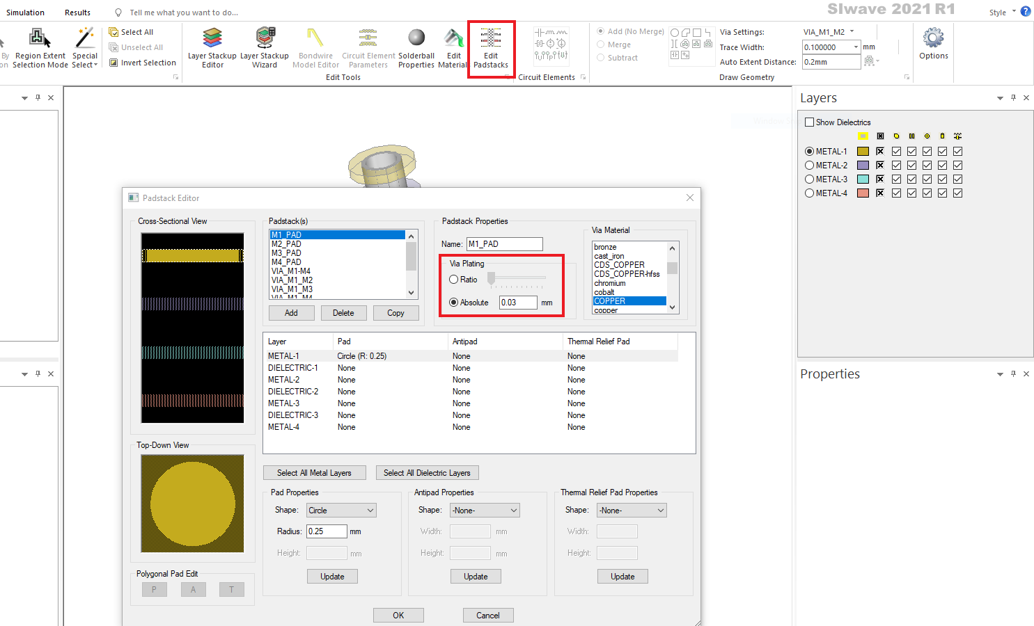
If you are asking how you can "validate" whether hollow or filled vias are exported to Q3D, to me, the obvious solution would be to open up Q3D after export and look at the vias. Also, the padstacks could be examined first in SIwave before exporting to Q3D to make sure the via plating is not 100%.
Best,
Manny
-
May 4, 2021 at 5:54 pm
-
May 5, 2021 at 3:15 pm
bsr
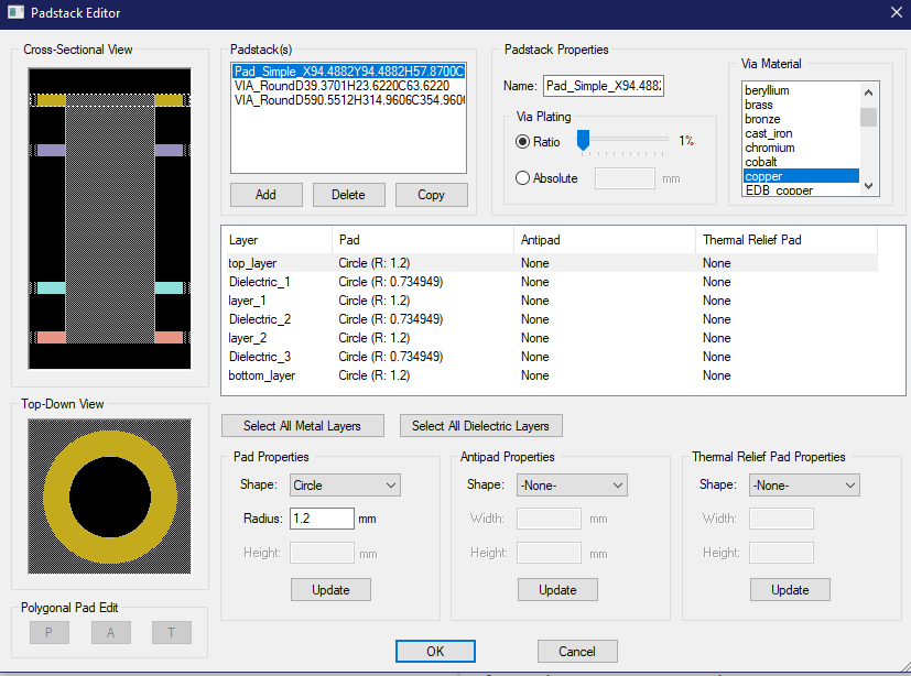
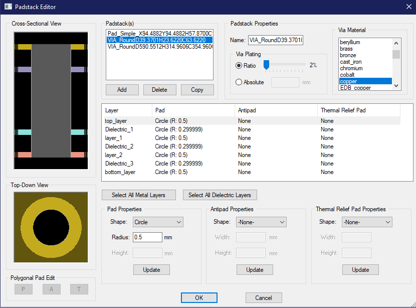
Subscribermanny Thanks for your inputs, which makes sense with illustration from Jackson !
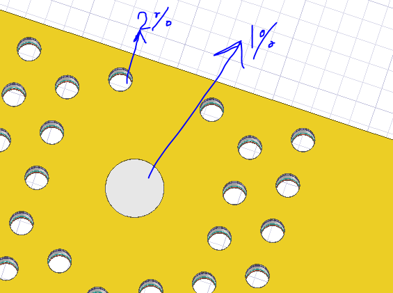
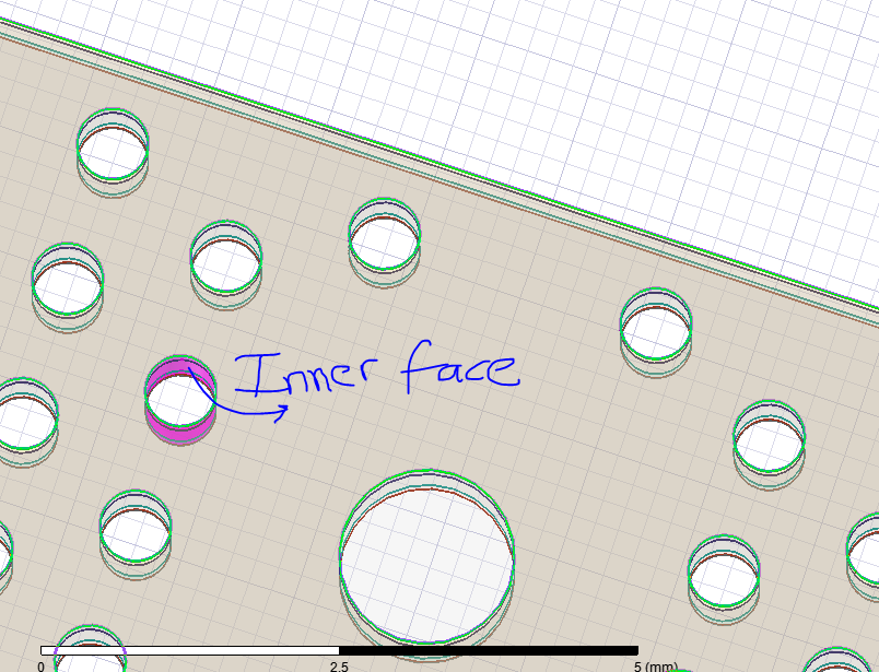
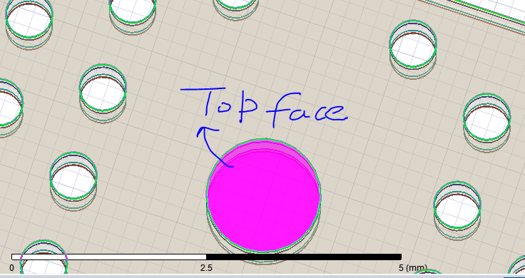
Jackson Thanks for the pictures, which helps a lot. I am noticing that Via Plating ratio has to be atleast 2% in order to properly see hollow vias in Q3D. I have tried 1% ratio, then once again I am unable to see hollow vias. I am attaching screenshot of the Q3D and SiWave workspaces.
If the vias are not hollow (the case with 1% plating in SiWave), then I am unable to select the inner face/ring of a the via within Q3D. In this case I can only select top and bottom faces, which in reality should be empty. In the second case with 2% plating, I can select the inner face. See attached images.
-
Viewing 8 reply threads
- The topic ‘ODB++ to SiWave and further to Q3D analysis Approach’ is closed to new replies.
Innovation Space


Trending discussions


Top Contributors


-
5159
-
1836
-
1387
-
1249
-
1021
Top Rated Tags


© 2026 Copyright ANSYS, Inc. All rights reserved.
Ansys does not support the usage of unauthorized Ansys software. Please visit www.ansys.com to obtain an official distribution.

