-
-
November 3, 2023 at 12:02 pm
Sungmin Yoon
SubscriberHello,
Currently I'm running CHARGE simulation to see charge transport at some semiconductor.
Acutally it is designated as semiconductor but its material parameters(for example, bandgap) which are those of some insulator.
My model's structure is "Metal-semiconductor-metal", ground bias at one metal, and negative sweep bias to the other end.
And "free charge" attribute in visualizer shows decreasing profile, gradually going to reaching to positive value.
According to description, free charge is 'p-n', so it means that electrons are being drained out.
Why is that happening, even though I applied negative bias?
Thanks,
Sungmin
-
November 3, 2023 at 9:36 pm
Amrita Pati
Ansys EmployeeHi Sugmin,
Would you be able to share a screenshot of the variation of free_charge?
Regards,
Amrita -
November 4, 2023 at 10:15 am
Sungmin Yoon
SubscriberThank you for your reply.
- This is my model. please ignore small lines / shadow on it. (proly due to graphical stuff)
2. these are Images of free_charge profile (0V, -3V, -5V, -7V, -10V, for convinence)
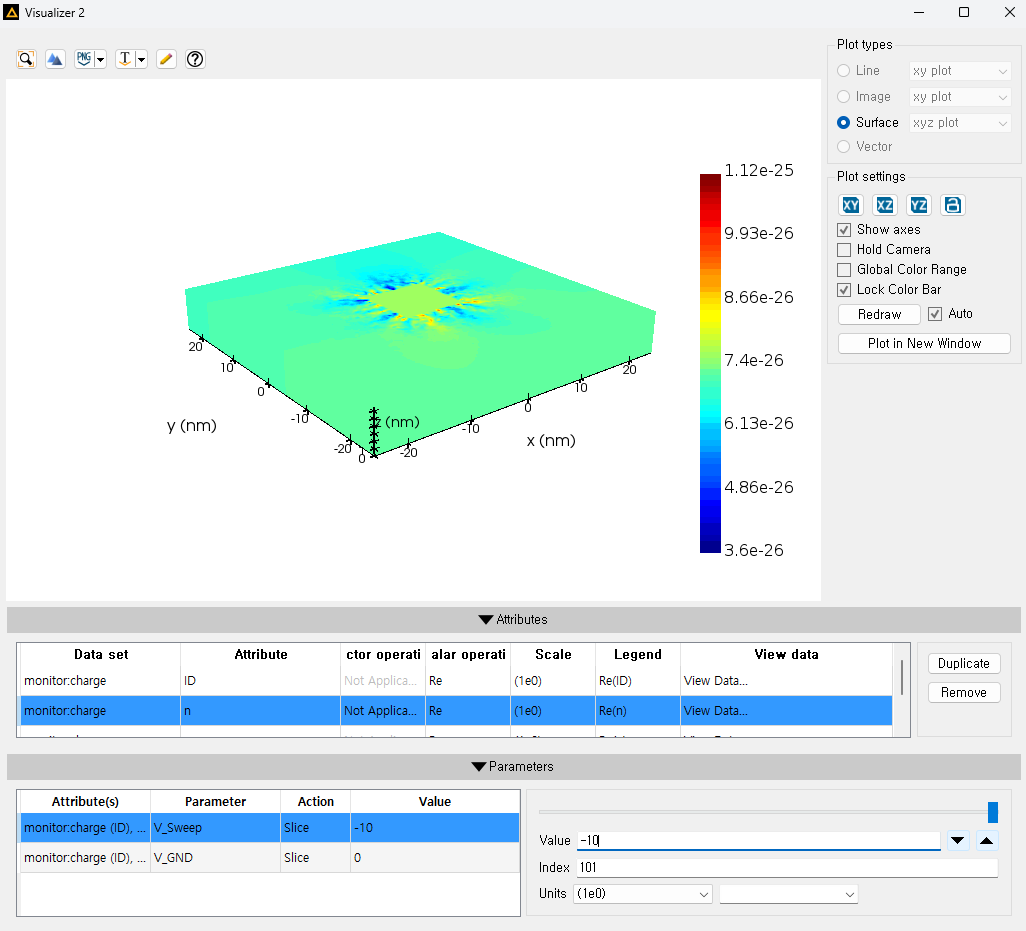
3. Images of 'n' attribute. It shows a bit more clear variation compared to free_charge (especially at the edge point of metal)
-
November 9, 2023 at 12:25 am
Amrita Pati
Ansys EmployeeHi Sungmin,
I am sorry about the late reply. I will have to speak to our CHARGE expert on this. He is on vacation currently and will be back at the start of next week. I will get back to you then. Also, I am wondering why you have the shadow lines. In my experience with FDTD, it happens when there are overlapping geometries. I believe the geometry here is pretty straightforward but I still want to double-check with you. Do you have any overlapping geometries? And if yes, are their mesh orders properly assigned?Regards,
Amrita-
November 20, 2023 at 3:53 am
Sungmin Yoon
SubscriberHello, Amrita.
Could you tell me if there are any updates?
Thanks,
Sungmin
-
-
November 9, 2023 at 1:16 am
Sungmin Yoon
SubscriberThank you for your information regarding charge expert.
To answer your question – nah, they are not overlapping. It is a stacked structure, like z=0~+6.5 nm for middle layer, z=6.5 ~ 7.5 nm for top metal contact. But thanks for checking. I’m new to ansys program so I was also wondered about that shadow. Could be due to my poor 3rd-gen ivybridge CPU. Whenever I change the view, shadow also changes(disappears/appears).
-
November 21, 2023 at 5:35 pm
Amrita Pati
Ansys EmployeeHi Sungmin,
Sorry for the delay, things have been very busy on our end. I have forwarded your questions to our CHARGE expert. We will come back to you with more updates.
Regards,
Amrita -
November 21, 2023 at 7:17 pm
Amrita Pati
Ansys EmployeeHi Sungmin,
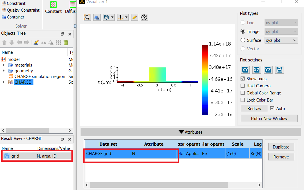
Thanks for your patience on this one! I heard back from my colleague. We notice that the concentration of carriers in your results is extremely low, especially if you compare it to a typical doped semiconductor. So, it is possible that the small variations that you are seeing are not actually accurate results but numerical artifacts. We would like to know more about what kind of effect you are trying to understand so that we can evaluate if CHARGE can simulate it accurately. Also, I would ask you to double check the simulation and make sure that the doping is correctly applied. For this, mesh the simulation region:
Then go the the "grid" result in CHARGE solver object and visualize the result "N" (which shows the doping level).
Regards,
Amrita-
November 22, 2023 at 1:23 pm
Sungmin Yoon
SubscriberHello, Amrita.
Thanks for the updates! To answer your question:
Actually it is a insulator(Si3N4) but I designated it as a semiconductor, and put literiture material properties. Cause I need to simulate Metal-Oxide-p type Si-Metal structured device to evaluate charge(electrons, holes) profile, as like this post. So the first thing that I wanted to know is whether CHARGE can simulate those behavior, throught the insulator, if I just assign them as semiconductor and filling up material properties. I got advised about that idea from here .
-
-
November 23, 2023 at 10:06 pm
Amrita Pati
Ansys EmployeeHi Sungmin,
Thanks for the additional details. That makes sense. So, I have used this approach in the past to look at electric field distributions in an insulator material. But I am not sure to what level we can trust the other results such as the carrier density. I have forwarded this question to the R&D. I will get back to you soon.
Regards,
Amrita-
November 24, 2023 at 12:05 am
Sungmin Yoon
SubscriberThanks for reply and fowarding to R&D team! Please keep me posted!
Best,
Sungmin
-
-
November 27, 2023 at 8:01 pm
Amrita Pati
Ansys EmployeeHi Sungmin,
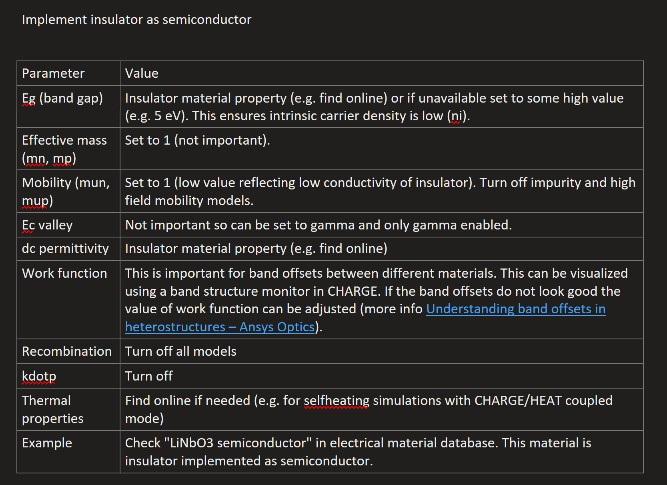
I heard back from the R&D team. With CHARGE we should be able to calcuate both the electric field and carrier densities accurately using this approach. Here is a screenshot of a table that the R&D team shared with me on defining insulators as semiconductors, you might find this useful:
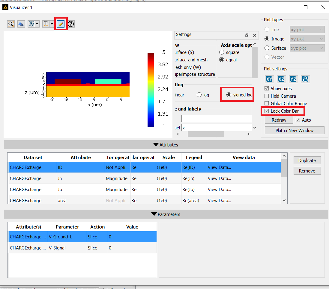
Now coming to this question, the carrier density is extremely low which is expected from an insulator. But this also makes it difficult to identify if the changes in the concentration is accurate or some numerical artifact. I would suggest you to change the scale to signed log, then lock the color bar, and then look at the carriers for different voltages. If you do this, does the change looks reasonable or unexpected?
Regards,
Amrita-
November 29, 2023 at 3:54 am
Sungmin Yoon
SubscriberHello, Amrita.
First of all, thank you for the table. Actually I've curioused about those properties and in case of Ec Vally I actually tested all the possible combinations and concluded that it dosen't matter that much ????. It is glad to see that it was right.
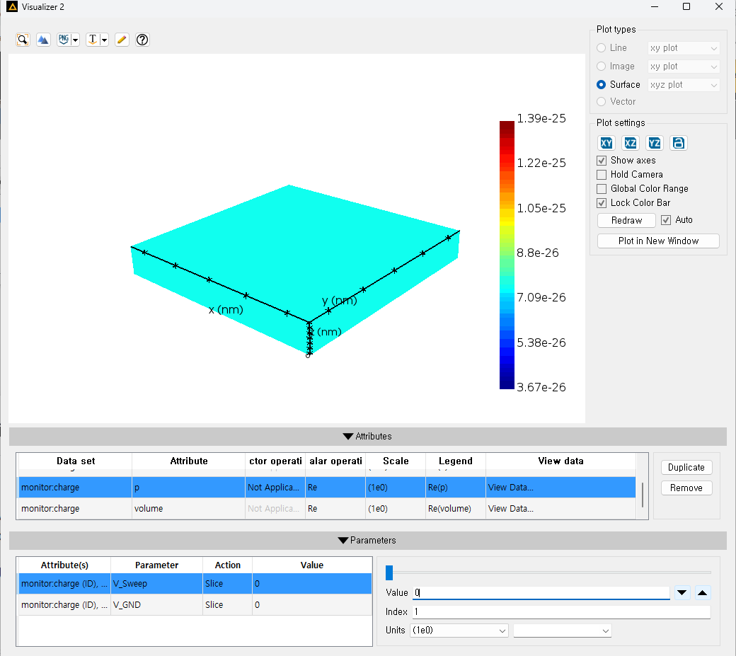
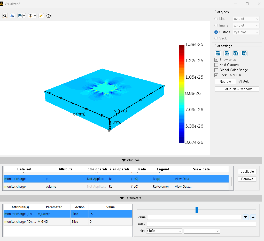
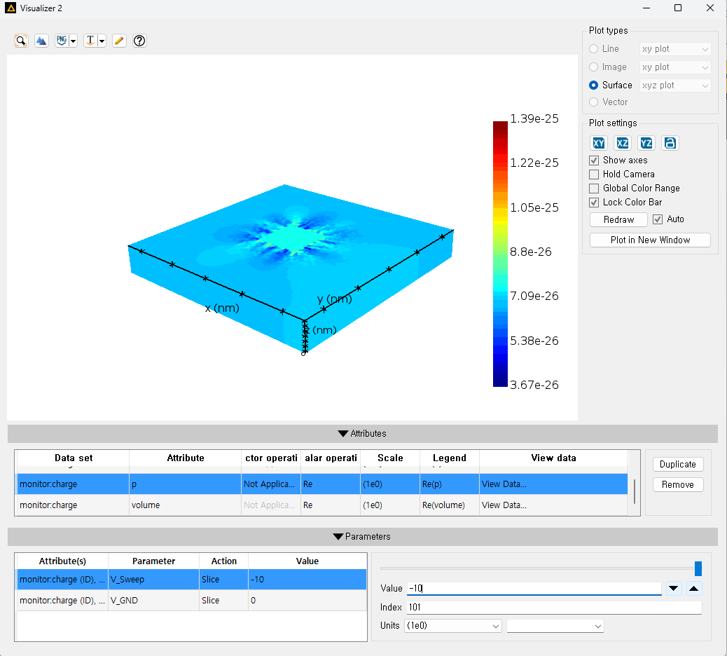
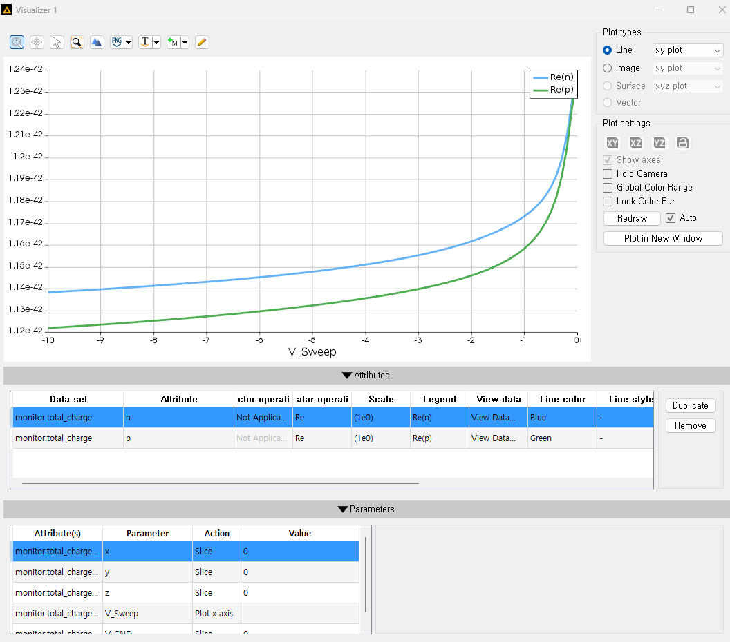
Bad news is - n attribute decreases as bias goes more negative - But the thing is, p attribute is also decreasing. Given that, I guess it is rather numerical error, like you mentioned.
Good news is - It's just a some kind of prior test, the real thing is the other one that you fowarded to R&D team. Thanks for your help.
Attached images in case of someone who has same/similar issue, as below:
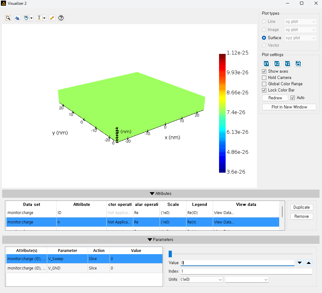
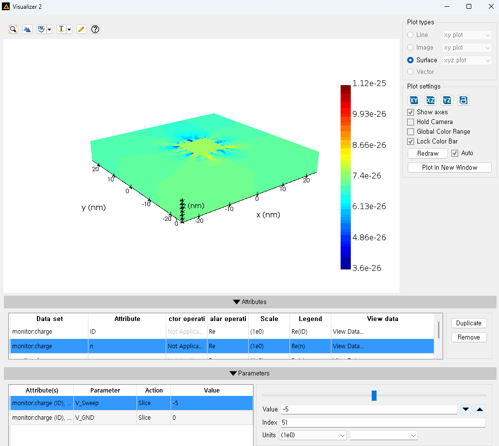
n attribute, 0V, -5V, -10V, respectively. Locked color bar with signed log, applying negative bias at the top part of object.
p attribute
Total charge profile
-
-
- The topic ‘Lumerical CHARGE) meaning of decreasing free charge’ is closed to new replies.


-
5734
-
1906
-
1419
-
1305
-
1021

© 2026 Copyright ANSYS, Inc. All rights reserved.


